

Improvement method for dislocation defect in embedded SiGe epitaxy
An embedded silicon germanium and epitaxy technology, applied in electrical components, semiconductor/solid-state device manufacturing, circuits, etc., can solve problems such as dislocation defects in silicon germanium epitaxy, and achieve the effects of ensuring germanium concentration, improving electrical properties, and increasing stress
- Summary
- Abstract
- Description
- Claims
- Application Information
AI Technical Summary
Problems solved by technology
Method used
Image

Examples
Embodiment Construction
[0025] The present invention will be further described below in conjunction with specific embodiment and accompanying drawing, set forth more details in the following description so as to fully understand the present invention, but the present invention can obviously be implemented in many other ways different from this description, Those skilled in the art can make similar promotions and deductions based on actual application situations without violating the connotation of the present invention, so the content of this specific embodiment should not limit the protection scope of the present invention.
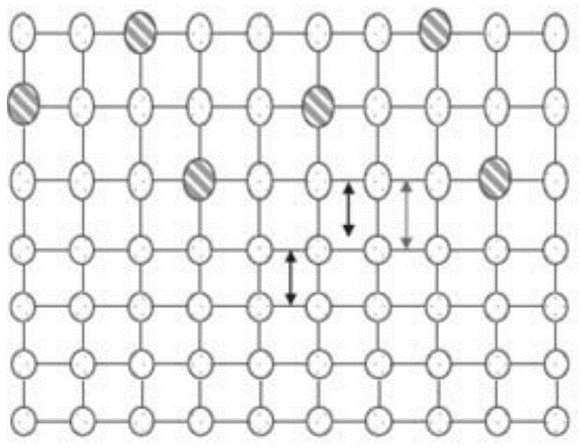
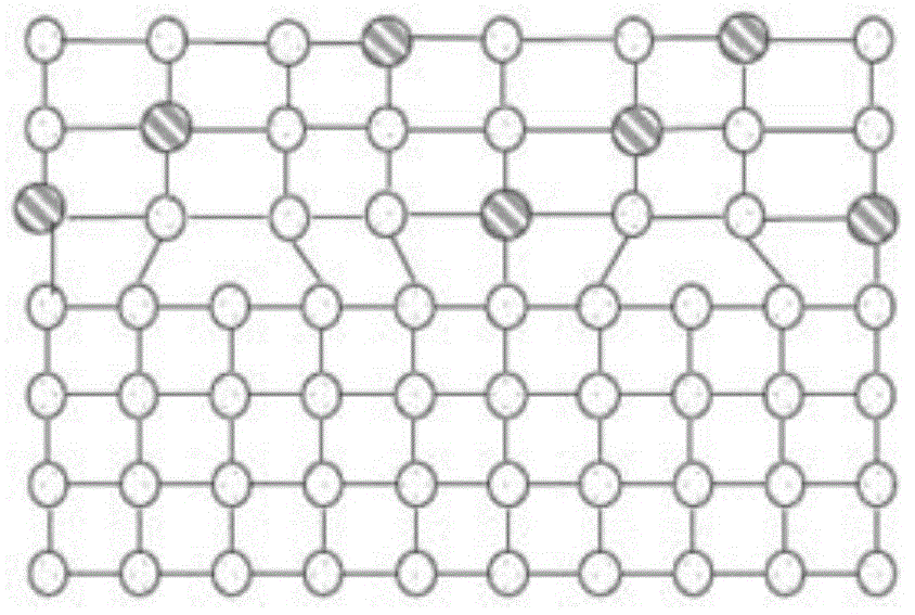
[0026] First, the inventors of the present case realized that in the embedded SiGe selective epitaxy process, there is a certain relationship between the germanium concentration and the thickness of the SiGe film. image 3 It is a schematic diagram of the Matthews-Blakeslee theoretical curve based on the silicon-germanium thin film in the method for improving dislocation defects...
PUM
 Abstract
Description
Claims
Application Information