A kind of LED product manufacturing method and LED product

A technology of LED chips and products, applied in semiconductor devices, electrical components, circuits, etc., can solve problems such as uneven light color, achieve the effects of simplifying the process flow, realizing controllable distribution, and preventing sedimentation

Inactive Publication Date: 2018-11-30
PEKING UNIV SHENZHEN GRADUATE SCHOOL
View PDF3 Cites 0 Cited by
  • Summary
  • Abstract
  • Description
  • Claims
  • Application Information

AI Technical Summary

Problems solved by technology

[0004] Aiming at the problem of uneven light color caused by the existing LED product manufacturing method, the application provides a LED product manufacturing method and LED product

Method used


Image

  • A kind of LED product manufacturing method and LED product
  • A kind of LED product manufacturing method and LED product
  • A kind of LED product manufacturing method and LED product

Examples


Embodiment 1

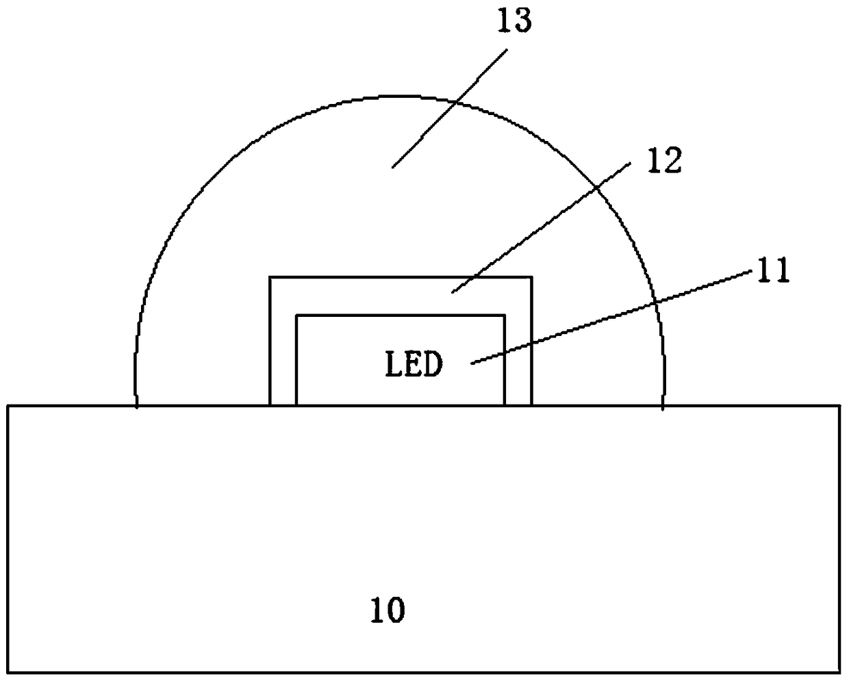
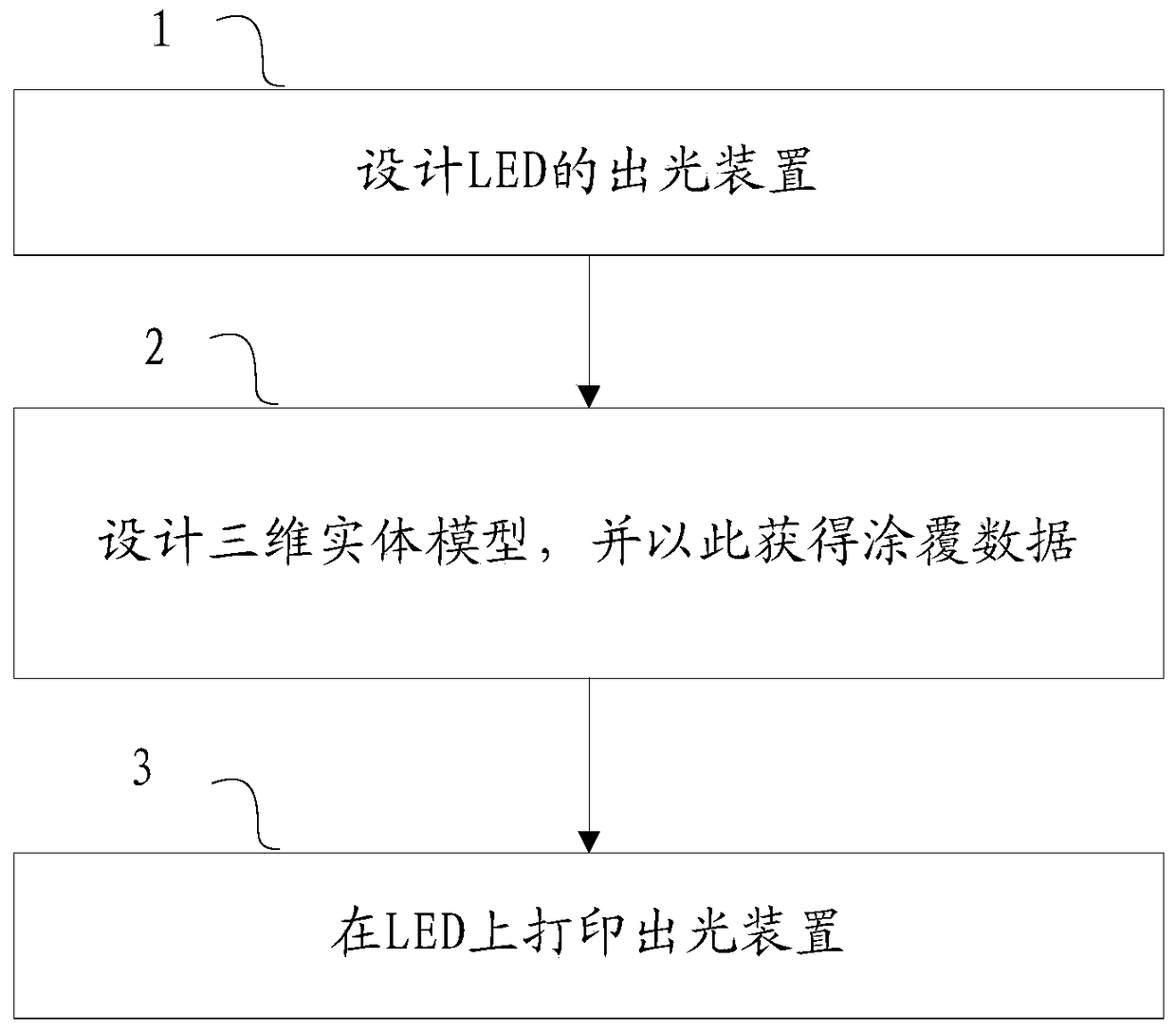
[0024] This example provides a LED product manufacturing method, the flow chart is as follows figure 2 As shown, it specifically includes the following steps.

[0025] Step 1: Design the light emitting device according to the light emitting requirements of LED products.

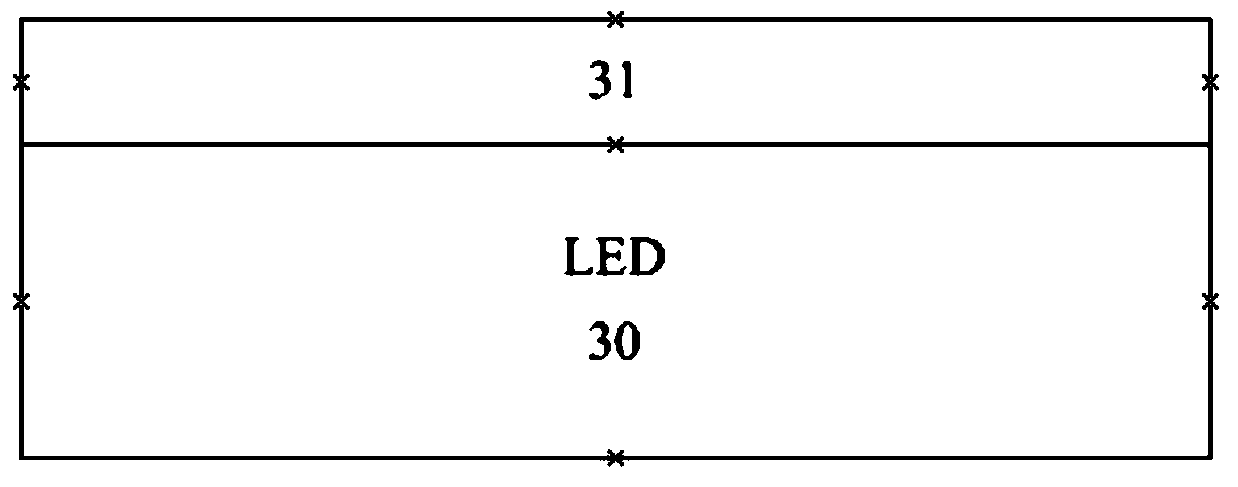
[0026] In order to make the light emitted by the LED chip output better, get the maximum utilization, and meet the design requirements in the lighting area, it is necessary to design the optical system of the LED. Among them, the design in the packaging process is called the primary optical design; the optical design outside the LED package is called the secondary optical design, also known as the secondary light distribution design, and the LED terminal product is completed after two designs Light mixing and homogenization. The color and energy conversion of the LED is realized by the phosphor layer, and the light mixing and uniform light of the LED are realized by the lens layer. In this embodiment, the...


PUM


Abstract

The invention discloses an LED product and a manufacturing method therefor. The manufacturing method comprises the steps of generating light-output apparatus design data according to a light emitting principle of an LED chip, a mechanism of exciting phosphor powder to generate white light by the LED chip, an optical design method and the like, wherein the light-output apparatus is used for absorbing exciting light and sending out excited light, and performing light-uniformity processing on the hybrid light of the excited light and the exciting light; generating a three-dimensional entity model according to the light-output apparatus design data, and processing the three-dimensional entity model by a discrete program to obtain 3D print data; controlling a 3D printer to stack the light-output apparatus according to 3D print data and predetermined materials, wherein the LED chip can be directly covered with the light-output apparatus, or can be separated from the light-output apparatus. By adoption of the LED product manufacturing method, controllable distribution of phosphor powder granules, phosphor powder layer patterns and lens layer patterns can be realized, so that the controllable distribution of light output is realized as well; and according to the manufacturing method, a phosphor powder coating technology, primary optical design and secondary optical design are organically combined together, so that the space structure of the lamp is effectively saved.

Description

technical field [0001] The invention relates to the lighting field, in particular to a method for manufacturing an LED product and an LED product. Background technique [0002] LED has many advantages such as energy saving, environmental protection and long life, especially when it is used in combination with solar cells and electromagnetic induction cells, it is a competitive green light source. The process of LED packaging to achieve white light is: when the blue light emitted by the LED chip is incident into the phosphor layer, since the blue light spectrum is within the excitation spectrum of the phosphor, the phosphor will strongly absorb the blue light, and a part of the absorbed blue light is converted into After the yellow phosphor is excited, it mixes with the blue light directly transmitted from the phosphor layer to form white light. Therefore, the coating method of the phosphor determines the quality of the light color of the white LED to a certain extent. If th...

Claims


Application Information

Patent Timeline
Patent Type & Authority Patents(China)
IPC IPC(8): H01L33/50H01L33/58
CPCH01L33/505H01L33/58H01L2933/0041H01L2933/0058
Inventor 刘葳张盛东
Owner PEKING UNIV SHENZHEN GRADUATE SCHOOL
Why Eureka
Try Eureka