

ICD (Internal Connection Defect) detection method for PCB
A detection method and inner layer technology, applied in circuit inspection/monitoring/correction, electrical connection formation of printed components, electrical components, etc., can solve the problem of high slicing level requirements, the influence of grinding debris on the detection results, and the difficulty in judging electroplating copper. Layer and inner layer copper ring, etc., to achieve strong practicability, improve detection efficiency, and save time.
- Summary
- Abstract
- Description
- Claims
- Application Information
AI Technical Summary
Problems solved by technology
Method used
Image

Examples
Embodiment Construction
[0019] Below, in conjunction with accompanying drawing and specific embodiment, the present invention is described further:
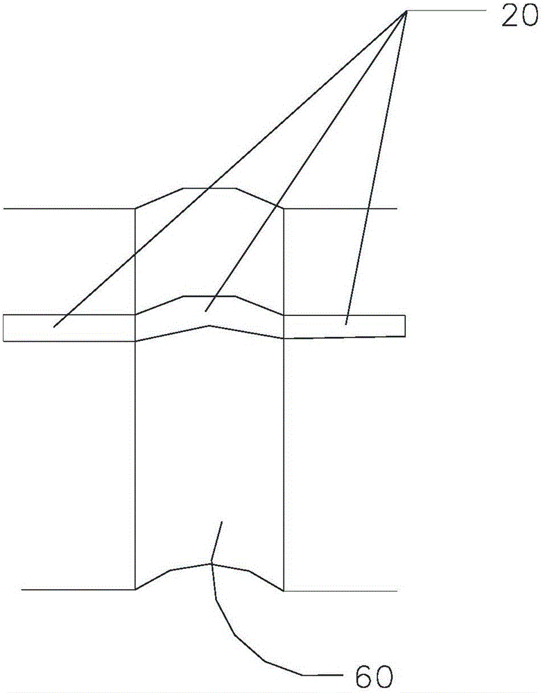
[0020] Such as Figure 1-3 As shown, a method for detecting interconnection defects in a PCB includes the following steps:
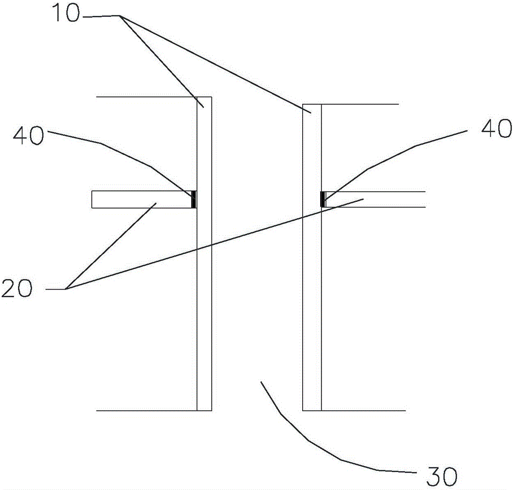
[0021] Step A: Make a vertical slice of the PCB sample, the schematic diagram of the slice section is as follows figure 1 As shown, use a metallographic microscope to observe whether there is a crack between the electroplated copper layer 10 and the inner layer copper ring 20 on the vertical section; if there is no crack, it means that there is no residual glue 40 between the electroplated copper layer 10 and the inner layer copper ring 20 , this situation does not affect the properties of the entire circuit, no further testing is required, and if there are cracks, proceed to the next step;
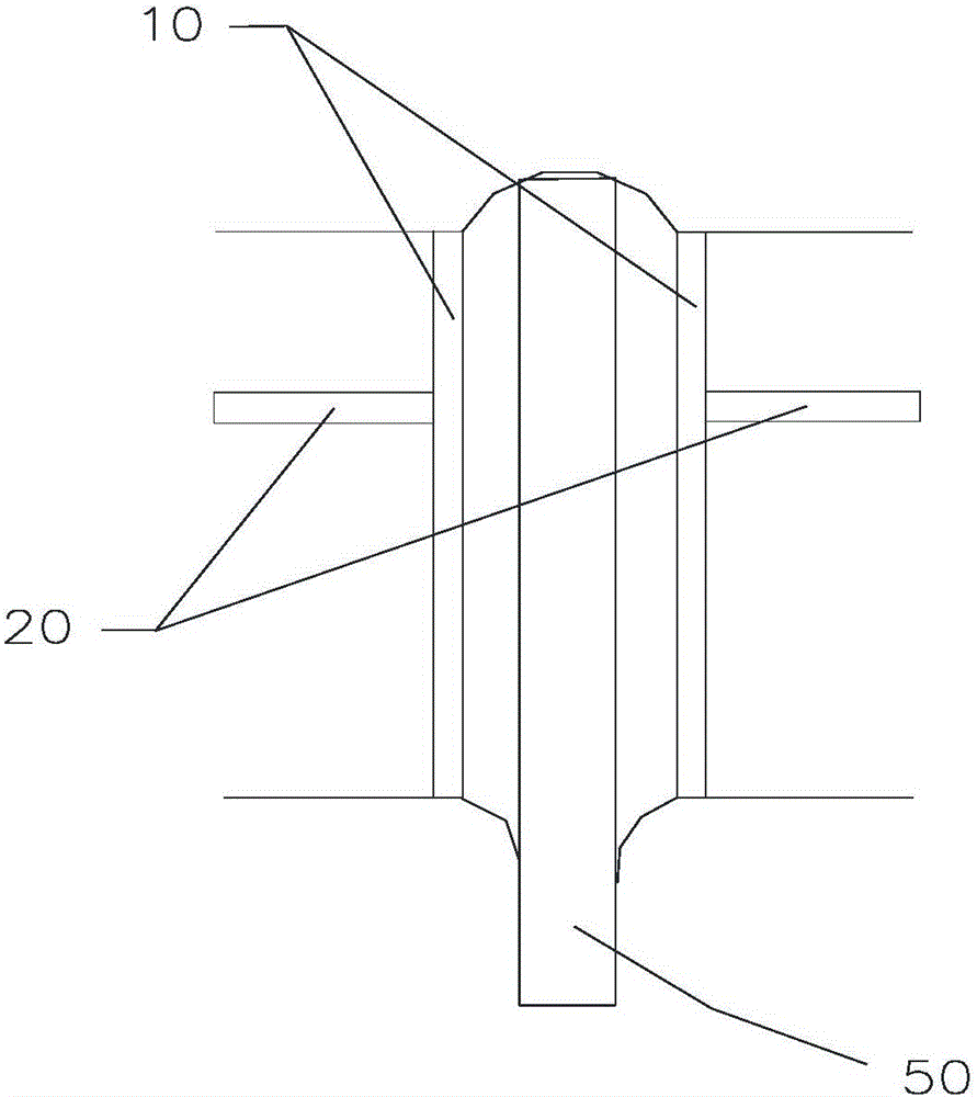
[0022] See figure 2 , Step B: If there is a crack, use an external force to separate the entire electroplated copper layer 10 from the i...
PUM
 Abstract
Description
Claims
Application Information