A method of calculating a wetting speed for Sn-based solder and a Cu substrate

A technology of wetting speed and calculation method, which is applied in the direction of analyzing materials, measuring devices, instruments, etc., can solve the problems of incompetence in fixed point, positioning, dimensional accuracy limitation, complicated process, etc., and achieve the improvement of service reliability, volume reduction, volume small effect

Inactive Publication Date: 2016-06-22
INST OF METAL RESEARCH - CHINESE ACAD OF SCI
View PDF6 Cites 4 Cited by
  • Summary
  • Abstract
  • Description
  • Claims
  • Application Information

AI Technical Summary

Problems solved by technology

However, traditional microstructure processing technologies such as photolithography are more complicated, and the dimensional accuracy is also limited. They are not capable of fixed-point, positioning, and single-piece fabrication of nano-microstructures of different shapes and sizes. Artificial microstructures are used to limit the wetted area of ​​metal liquid reaction. research has not yet been reported in the literature

Method used


Image

  • A method of calculating a wetting speed for Sn-based solder and a Cu substrate
  • A method of calculating a wetting speed for Sn-based solder and a Cu substrate
  • A method of calculating a wetting speed for Sn-based solder and a Cu substrate

Examples


Embodiment 1

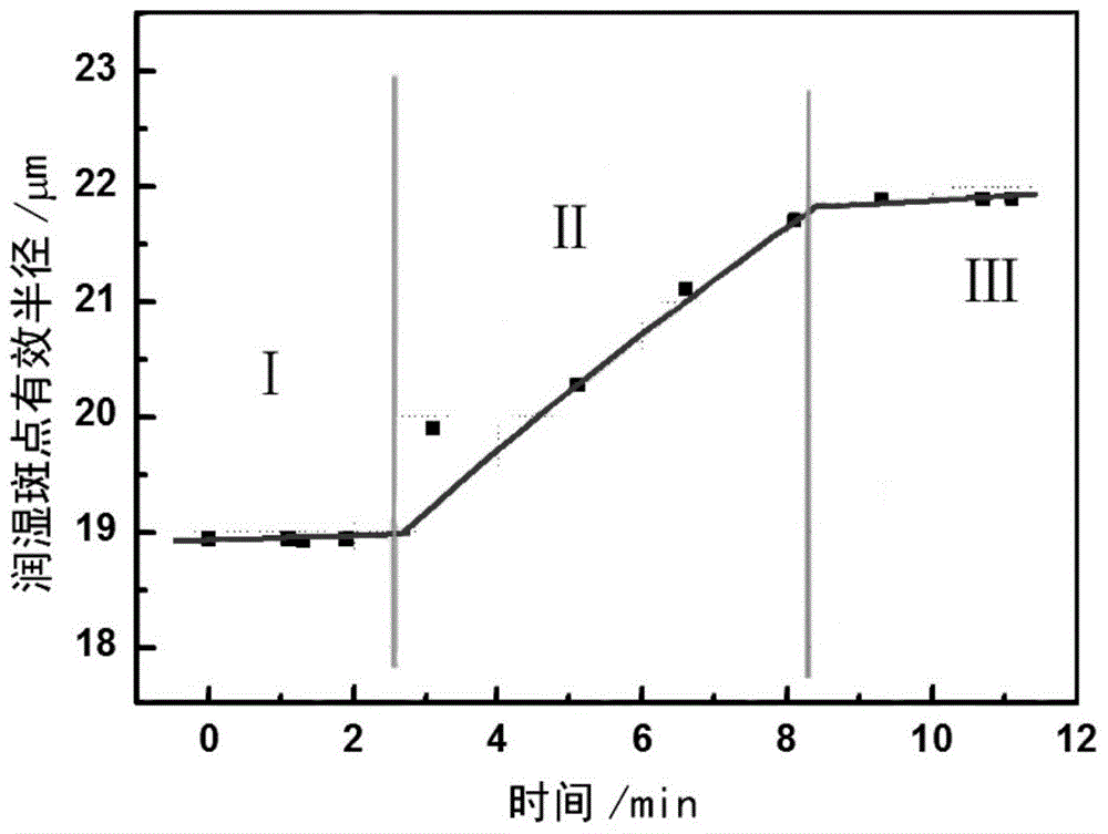
[0034] In this embodiment, a high-temperature metallographic microscope is used to observe the wetting process of Sn-based solder on the Cu substrate in situ and calculate the wetting speed. The specific process is as follows:

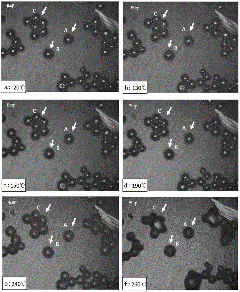
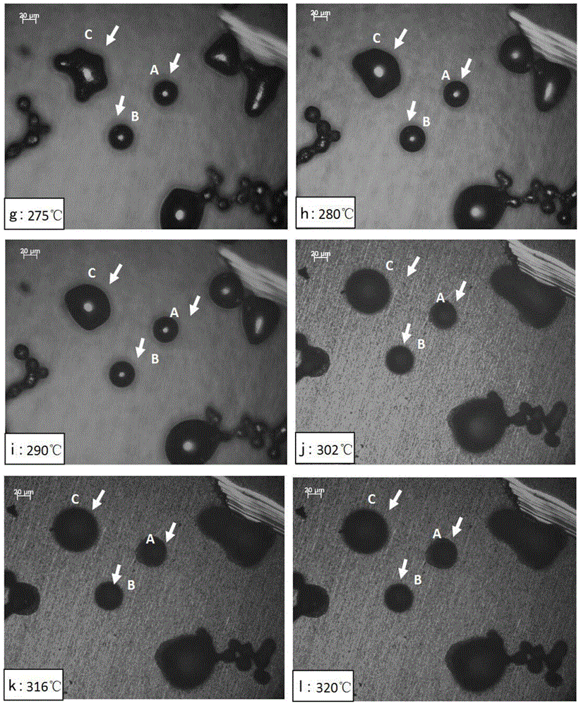
[0035] 1. Wetting process of solder on copper sheet and morphology of wetting spots

[0036] Put the Sn-based solder on the copper sheet, then place the sample in the hot stage of LinkamTHMS600, put the hot stage on the Axiophoto2imageE upright microscope, and pass 99.999% argon gas in the hot stage. The sample is heated up, the heating rate is set according to the melting of the solder, and the in-situ wetting process of the Sn-based solder on the Cu substrate is observed through a microscope. figure 1 It is the wetting process of Sn-based solder on the Cu substrate. It can be seen from the figure that some Sn particles are connected together, and some exist alone. The A and B particles that exist alone are the objects of observation and analysis. . ...


PUM


Abstract

The invention discloses a method for calculating the wetting speed of Sn-based solder and Cu matrix, belonging to the technical field of solder wettability. Firstly, the wetting behavior of tin solder on the copper substrate microstructure is observed by a high-temperature metallographic microscope, and the time-image area relationship curve is established after collecting the image, and the curve of the effective radius of the wetting spot changing with time can be obtained, and the effective radius varies with time. The time-varying functional relationship from which the rate at which the wetted spot wets under the experimental conditions is calculated. The method of the invention can establish an image acquisition and calculation method of wetting reaction speed for solder wetting spots of any shape, and provides an important basis for solving the wetting control of Sn solder in micro-nano structures and reducing the size and spacing of micro-connections.

Description

technical field [0001] The invention relates to the technical field of solder wettability, in particular to a method for calculating the wetting speed of Sn-based solder and Cu substrate. Background technique [0002] Tin soldering is the most widely used joining process in modern microelectronics technology. The International Semiconductor Technology Roadmap sets out the goal of developing high-density connections. Improving the connection density, on the one hand, helps to realize the miniaturization and weight reduction of electronic devices; The length of the inner wire reduces the resistance, reduces the calorific value, enhances the heat dissipation capability, and improves the service reliability of the device. [0003] In a limited space, to accommodate enough solder joints without bridging, and to realize the minimum size of reliable connection is a problem that engineers and scientific researchers are concerned about at present. Studying the wetting phenomenon o...

Claims


Application Information

Patent Timeline
IPC IPC(8): G01N13/00
Inventor 盖秀颖刘金柱杨飞雪
Owner INST OF METAL RESEARCH - CHINESE ACAD OF SCI
Why Eureka
Try Eureka