Thick copper plate for different types of circuit boards and production method for circuit board

A production method and technology of thick copper plate, applied in the direction of multi-layer circuit manufacturing, printed circuit manufacturing, circuit lamination, etc., can solve the problem that the expansion and shrinkage of copper plate and FR4 substrate is not easy to control, and it is impossible to arrange and combine multiple circuit boards. , increase production costs and other issues, to achieve the effect of reducing production process and production time, avoiding sheet material expansion and shrinkage, and saving production costs

Active Publication Date: 2016-06-22
南通胜宏科技有限公司
View PDF6 Cites 7 Cited by
  • Summary
  • Abstract
  • Description
  • Claims
  • Application Information

AI Technical Summary

Problems solved by technology

In the traditional circuit board processing, in order to achieve the basic edge-wrapping effect of FR4, it is necessary to open a common FR4 substrate in advance, hollow out the FR4 substrate according to the shape of the copper board, and then cut out the shape of the copper board separately, and finally the completed The copper plate is embedded into the FR4 substrate for lamination. This method can only be produced by a single circuit board, and multiple circuit boards cannot be typed and combined. The production efficiency is low and the process is long, and each board needs to waste a common FR4 substrate. Sheet metal increases production costs, and the expansion and contraction of copper plates and FR4 substrates is not easy to control

Method used


Image

  • Thick copper plate for different types of circuit boards and production method for circuit board
  • Thick copper plate for different types of circuit boards and production method for circuit board
  • Thick copper plate for different types of circuit boards and production method for circuit board

Examples


Embodiment Construction

[0023] In order to allow those skilled in the art to better understand the technical solutions of the present invention, the present invention will be further described below in conjunction with the accompanying drawings.

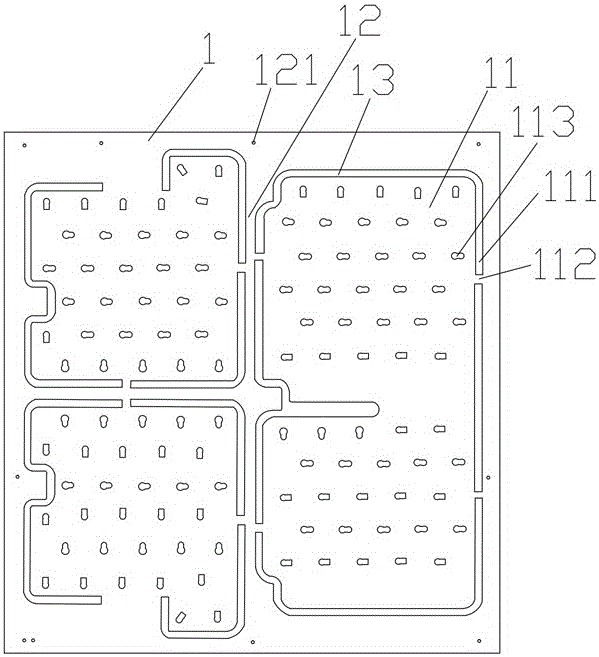
[0024] Such as figure 1 As shown, a thick copper plate of a different type of circuit board includes a thick copper plate 1 with a thickness of 1.0-1.2mm in a square structure. In order to improve the utilization rate of the thick copper plate and save production raw materials, the thick copper plate 1 is provided with a plurality of thick copper plate units 11 corresponding to different types of circuit boards and a connection area 12 connecting each thick copper plate unit, through the connection area 12 The connection makes each thick copper plate unit connected to the whole thick copper plate and has an integrated structure. The outer side of each thick copper plate unit 11 is provided with a rim 111 and a connecting position 112, and the gong edge 111...


PUM

PropertyMeasurementUnit
Lengthaaaaaaaaaa
Widthaaaaaaaaaa
Widthaaaaaaaaaa

Abstract

The invention discloses a thick copper plate for different types of circuit boards and a production method for the circuit board. The thick copper plate is of a square structure, and a thick copper plate unit and a connecting area are arranged on the thick copper plate; a gong side and a connecting position are arranged at the outer side of each thick copper plate unit, and each thick copper plate unit is connected to a connecting part through the connecting position; a plurality of locating holes are arranged in the connecting area and are located on a frame of the thick copper plate. The invention also discloses a production method for the circuit board. According to the thick copper plate for different types of circuit boards and the production method for the circuit board, the utilization rate of the board and the production efficiency of the circuit board are effectively improved, the production cost is saved, the waste of the production raw materials is reduced and the fast batch production is realized; meanwhile, the circuit board is directly formed in the thick copper plate and then composing and laminating are carried out without taking an FR4 substrate as a lag, so that the expansion problem of materials of the copper plate and the FR4 substrate after laminating is avoided, the use of the FR4 substrate is reduced, the production process and the production time are reduced, an effect of coating the FR4 substrate on the copper plate is better realized, and the circuit board is protected.

Description

technical field [0001] The invention belongs to the technical field of circuit board production, and in particular relates to a thick copper plate of different types of circuit boards and a method for manufacturing the circuit board. Background technique [0002] With the continuous development of the circuit board industry, circuit boards for various purposes also appear. In recent years, due to the increasing international and domestic attention to environmental protection issues and the adjustment of national strategies, the rapid development of the new energy electric vehicle and electric vehicle industry has been promoted and the application in the new energy electric vehicle and electric vehicle industry for Circuit board technology for high-current and high-voltage battery protection has also grown rapidly. [0003] Since the power battery protection circuit board needs to carry large current and high voltage, ordinary circuit boards can no longer meet this requireme...

Claims


Application Information

Patent Timeline
IPC IPC(8): H05K1/02H05K3/46
CPCH05K1/0298H05K3/4602H05K2203/06
Inventor 施世坤何艳球李雄杰张亚锋
Owner 南通胜宏科技有限公司
Why Eureka
Try Eureka