Semiconductor device and method for manufacturing the same

A manufacturing method and semiconductor technology, which can be used in semiconductor/solid-state device manufacturing, semiconductor devices, electric solid-state devices, etc., and can solve problems such as uneven film thickness of the base film

Inactive Publication Date: 2016-06-29
MITSUBISHI ELECTRIC CORP
View PDF6 Cites 3 Cited by
  • Summary
  • Abstract
  • Description
  • Claims
  • Application Information

AI Technical Summary

Problems solved by technology

[0008] In Patent Document 1, the technique of forming the Ni plating film is disclosed on the basis of reducing the crystal grains of the base film for growth of the Ni plating film and making the base film have a specific crystallographic orientation. The surface of the growing basement membrane, such as figure 1 As shown in Fig. 1 , although slight steps remain, it is conceivable that the film thickness of the base film becomes uneven when the degree of remaining steps of the base film is large.

Method used


Image

  • Semiconductor device and method for manufacturing the same
  • Semiconductor device and method for manufacturing the same
  • Semiconductor device and method for manufacturing the same

Examples


Embodiment Construction

[0031]

[0032] Before describing the embodiments according to the present invention, problems in forming lead-out electrodes in a general vertical power device will be described.

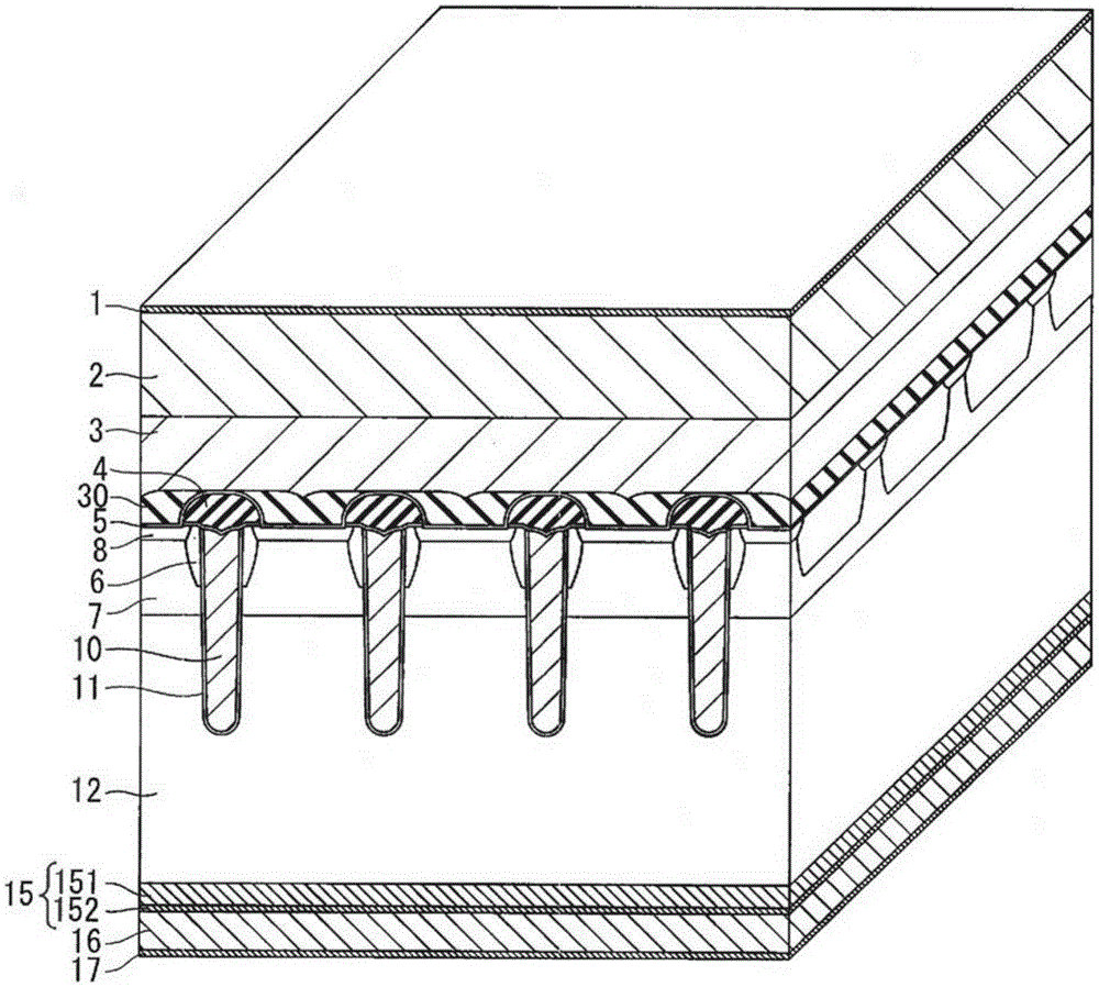
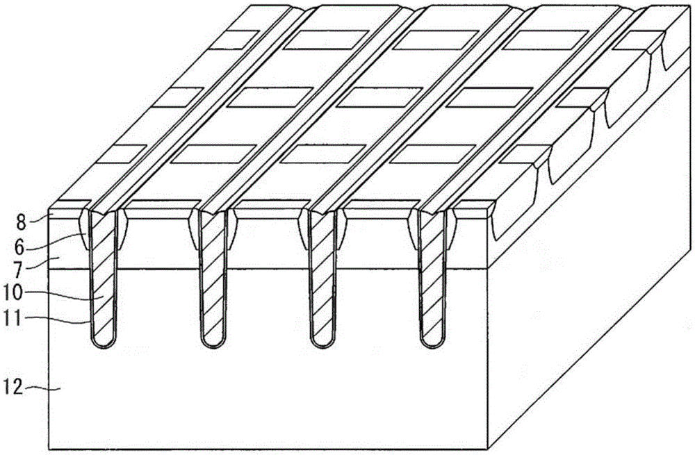
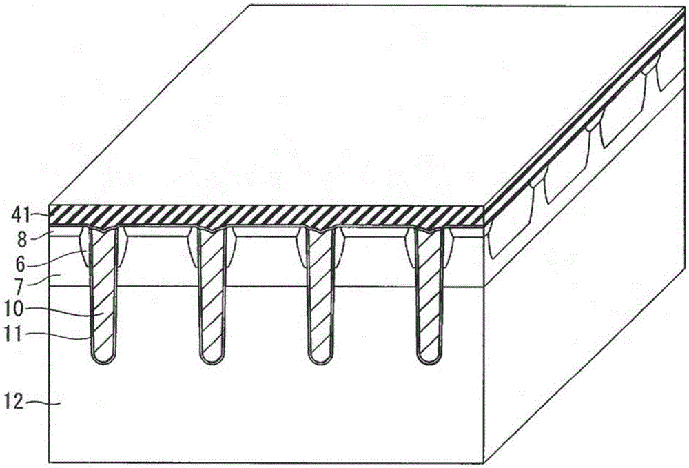
[0033] Figure 12 It is a cross-sectional view showing a partial structure of a trench gate type MOS transistor. In addition, this MOS transistor will be described as an N-channel type MOS transistor. Such as Figure 12 As shown, a P-type impurity layer 7 (body region) is provided on one main surface (upper main surface) side of an N-type semiconductor substrate 12, and a P-type impurity layer 8 (body region) is selectively provided in the surface of the impurity layer 7 ( contact area). Further, a plurality of trench gate electrodes 10 are provided so as to penetrate the impurity layer 8 and the impurity layer 7 and reach into the semiconductor substrate 12 .

[0034] The surface of trench gate electrode 10 is covered with gate oxide film 11 (gate insulating film), and N-type impurity layer ...


PUM


Abstract

A semiconductor device includes: a semiconductor substrate; a plurality of trench gate electrodes that have a stripe shape in plan view and are located in parallel with each other at an interval; a gate insulating film located on surfaces of the trench gate electrodes; a first impurity layer located in an upper layer portion of the semiconductor substrate; a second impurity layer that is selectively located in a surface of the first impurity layer and is in contact with the gate insulating film; an interlayer insulating film that is located so as to cover upper portions of the trench gate electrodes and an upper portion of the second impurity layer, projects on the semiconductor substrate, and has a stripe shape in plan view; and a planarized buried film of metal that is buried in portions between projecting portions of the interlayer insulating film on the semiconductor substrate.

Description

technical field [0001] The present invention relates to a semiconductor device, and in particular, to an improvement in a contact structure between a bonding electrode and a lead-out electrode through which a main current flows in a power semiconductor device. Background technique [0002] From the perspective of protecting the global environment, in order to efficiently use energy and seek miniaturization and higher output of power systems, it is required to increase the current density of power semiconductor devices (power devices) mounted in power systems. In addition, along with an increase in current density, improvement in heat dissipation performance and reduction in resistance of electrode junctions are sought. [0003] In order to achieve the above objects, in power devices, especially vertical type power devices in which the main current flows in a direction perpendicular to the main surface of the semiconductor substrate, a structure is being standardized in which...

Claims


Application Information

Patent Timeline
Patent Type & Authority Applications(China)
IPC IPC(8): H01L29/78H01L29/739H01L21/336H01L21/331H01L29/40H01L21/28
CPCH01L29/40H01L29/401H01L29/66348H01L29/66666H01L29/7397H01L29/7827H01L29/66734H01L29/41741H01L29/7813H01L29/0696H01L29/45H01L2224/33181H01L2224/32245H01L2224/06181
Inventor 赤尾真哉
Owner MITSUBISHI ELECTRIC CORP
Why Eureka
Try Eureka