
Wafer processing laminate, temporary adhesive material for wafer processing, and method for manufacturing thin wafer

一种晶片加工、晶片的技术,应用在晶片加工体领域,能够解决剥离长的时间、难以应用制造工艺等问题,达到耐热性高、耐性优异、膜厚均匀的效果

Active Publication Date: 2016-07-06
SHIN ETSU CHEM CO LTD
View PDF7 Cites 5 Cited by
  • Summary
  • Abstract
  • Description
  • Claims
  • Application Information

AI Technical Summary

Problems solved by technology

Therefore, it takes a very long time to peel off, and it is difficult to apply it to the actual manufacturing process

Method used


Image

  • Wafer processing laminate, temporary adhesive material for wafer processing, and method for manufacturing thin wafer
  • Wafer processing laminate, temporary adhesive material for wafer processing, and method for manufacturing thin wafer
  • Wafer processing laminate, temporary adhesive material for wafer processing, and method for manufacturing thin wafer

Examples


Embodiment

[0172] Hereinafter, although an Example and a comparative example are shown and this invention is demonstrated more concretely, this invention is not limited to these Examples.

Synthetic example 1

[0174] In a flask equipped with a stirrer, a thermometer, a nitrogen substitution device and a reflux cooler, 43.1 g of 9,9'-bis(3-allyl-4-carboxyphenyl)fluorene (M-1) was charged, and the average structural formula ( 29.5 g of organohydrogensiloxane represented by M-3), 135 g of toluene, and 0.04 g of chloroplatinic acid were heated up to 80°C. Then, 17.5 g of 1,4-bis(dimethylsilyl)benzene (M-5) was dripped in the flask over 1 hour. At this time, the temperature in the flask rose to 85°C. After completion of the dropping, aging was carried out at 80° C. for 2 hours, toluene was distilled off, and 80 g of cyclohexanone was added to obtain a resin solution in which the resin solid content concentration was 50% by mass of cyclohexanone as a solvent. The molecular weight of the resin fraction of the solution was measured by gel permeation chromatography (GPC), and the weight average molecular weight in terms of polystyrene was 45,000. Further in the described resin solution of ...

Embodiment 1

[0202]A silicon wafer (thickness: 725 μm) with a diameter of 200 mm and a copper post with a height of 10 μm and a diameter of 40 μm formed on the entire surface was spin-coated with the above (C-1) solution, and heated at 150° C. for 3 minutes on a hot plate to make The material corresponding to the (C) layer was formed into a film with the film thickness shown in Table 1 on the bump formation surface of the wafer. Then, a solution (A-1) of a thermosetting siloxane polymer corresponding to the (A) layer was formed on the (C) layer on the silicon wafer by spin coating, and the film thicknesses in Table 1 were formed. Then, it was further heated on a hot plate at 150° C. for 3 minutes. On the other hand, using a glass plate with a diameter of 200 mm (thickness: 500 μm) as a support, the polymer solution (B-1) corresponding to the (B) layer was first spin-coated on the support, and using a heating plate By heating at 150° C. for 5 minutes, the film thickness described in Table ...


PUM

PropertyMeasurementUnit
viscosityaaaaaaaaaa
glass transition temperatureaaaaaaaaaa
viscosityaaaaaaaaaa

Abstract

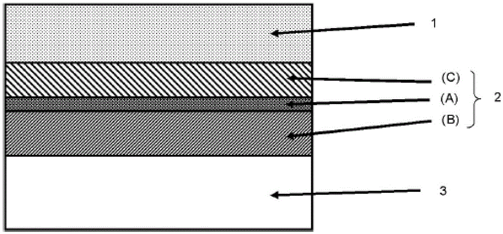
The present invention provides a wafer processing laminate, a temporary adhesive material for a wafer processing, and a method for manufacturing a thin wafer using the same, which facilitate temporary adhesion, allow to form a layer with uniform film thickness on a heavily stepped substrate, are highly compatible with steps of forming a TSV and forming a wiring on the back surface of the wafer, have excellent resistance to a thermal process for wafer such as CVD (chemical vapor deposition), enable easy delamination, and are capable of increasing productivity of thin wafers. To accomplish the objects, the present invention provides a temporary adhesive material for a wafer processing, the temporary adhesive material being used for temporarily bonding a support to a wafer having a circuit-forming front surface and a back surface to be processed, comprising a complex temporary adhesive material layer that has a first temporary adhesive layer composed of a thermosetting siloxane polymer layer (A), a second temporary adhesive layer composed of a thermosetting polymer layer (B) laminated on one surface of the first temporary adhesive layer, and a third temporary adhesive layer composed of a thermoplastic resin layer (C) laminated on the other surface of the first temporary adhesive layer.

Description

technical field [0001] The present invention relates to a wafer processing body capable of efficiently obtaining a thin wafer, a temporary adhesive material for wafer processing, and a method for manufacturing a thin wafer. Background technique [0002] In order to achieve further high density and large capacity, three-dimensional semiconductor structures have become necessary. The three-dimensional packaging technology refers to a semiconductor manufacturing technology that thins a semiconductor chip, further uses through silicon vias (through silicon vias, TSVs) to connect the chips, and stacks them into multiple layers. In order to realize this technique, the steps of reducing the thickness of the substrate on which the semiconductor circuit is formed by grinding the non-circuit-formed surface (also referred to as the "back surface"), and further forming electrodes including TSVs on the back surface are required. Conventionally, in the backside grinding process of a sili...

Claims


Application Information

Patent Timeline
Patent Type & Authority Applications(China)
IPC IPC(8): C09J183/07C09J183/04C09J7/02C09J7/10
CPCC09J7/35C09J183/04C08L2205/025C08L2205/03C08L83/04C08L61/20C08K5/13C08K5/1515C08G77/52C08G77/12C08G77/20H01L21/6835H01L2221/68327H01L2221/6834H01L2221/68381C08K5/56C08L83/00C09J7/10C09J2203/326C09J2483/00C09J2301/208C09J2301/304B32B7/12B32B2250/02B32B2255/26B32B2457/14H01L21/304H01L21/30625H01L21/6836
Inventor 田边正人菅生道博安田浩之田上昭平加藤英人
Owner SHIN ETSU CHEM CO LTD
Learn More