Wafer processing body, temporary adhesive material for wafer processing, and method

A kind of adhesive material, temporary technology, applied in the direction of semiconductor/solid-state device manufacturing, polymer adhesive additive, film/sheet without carrier, etc., can solve the problems of cleaning and removability, difficult to apply production process, long peeling Time and other issues, to achieve good CVD resistance, shorten the bonding time, easy to crack the effect

Pending Publication Date: 2022-05-20
SHIN ETSU CHEM IND CO LTD
View PDF12 Cites 0 Cited by
  • Summary
  • Abstract
  • Description
  • Claims
  • Application Information

AI Technical Summary

Problems solved by technology

Therefore, it takes a very long time to peel off, and it is difficult to apply to the actual production process
In addition, after peeling off, it takes a long time to clean the silicone adhesive remaining on the substrate as residue, which also has problems in cleaning removability.
On the other hand, in the bonding process, heating at about 150°C is required when heat-curable silicone is used, and warpage of the wafer becomes a problem especially when heating on a hot plate.
Therefore, it is intended to suppress warpage of the wafer by performing bonding at a low temperature, but in this case, there is a problem that it takes a long time to complete curing.

Method used


Image

  • Wafer processing body, temporary adhesive material for wafer processing, and method
  • Wafer processing body, temporary adhesive material for wafer processing, and method
  • Wafer processing body, temporary adhesive material for wafer processing, and method

Examples


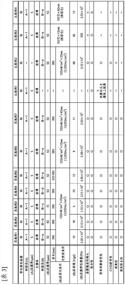
Embodiment 1~7 and comparative example 1~4

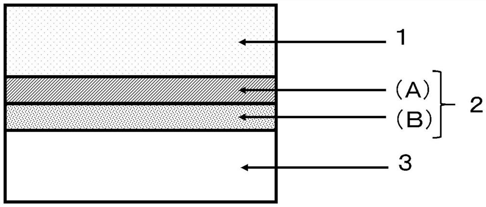
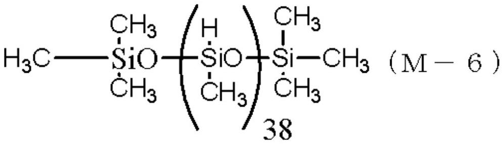
[0191] After the material (A-1) corresponding to the (A) layer was spin-coated on a silicon wafer (thickness: 725 μm) with a diameter of 200 mm and a copper pillar with a height of 10 μm and a diameter of 40 μm formed on the entire surface, the By heating at 150° C. for 5 minutes, the layer (A) was formed into a film with the film thickness shown in Table 3 on the bump formation surface of the wafer. On the other hand, a glass plate with a diameter of 200 mm (thickness: 500 μm) was used as a support, and a solution of a photocurable silicone composition corresponding to layer (B) was spin-coated on the support, and then placed on a hot plate. By heating at 70°C for 2 minutes, the layer (B) was formed on the support with the film thickness shown in Table 3. Using EVG's wafer bonding device EVG520IS, at 25°C, 10 -3 Under the conditions of below mbar and a load of 5kN, the silicon wafer with the thermoplastic resin layer (A) and the glass plate with the photocurable siloxane pol...

Embodiment 8~10

[0216] After the material (A-1) corresponding to the (A) layer was spin-coated on a silicon wafer (thickness: 725 μm) with a diameter of 200 mm and a copper pillar with a height of 10 μm and a diameter of 40 μm formed on the entire surface, the By heating at 150° C. for 5 minutes, the (A) layer was formed into a film with the film thickness shown in Table 4 on the bump formation surface of the wafer. On the other hand, a solution of a photocurable silicone composition corresponding to the (B) layer was spin-coated on a silicon wafer with a diameter of 200 mm (thickness: 500 μm) used as a support, and then heated on a hot plate at 70° C. It heated for 2 minutes, and formed (B) layer on a support body with the film thickness shown in Table 4. Next, the (B) layer was irradiated with light under the conditions shown in Table 4 using a surface irradiation type UV-LED (wavelength 365 nm) irradiator. Using EVG's wafer bonding device EVG520IS, at 40°C, 10 -3 The silicon wafer with t...


PUM

PropertyMeasurementUnit
widthaaaaaaaaaa
glass transition temperatureaaaaaaaaaa
viscosityaaaaaaaaaa

Abstract

The present invention is a temporary bonding material for wafer processing, which is used for temporarily bonding a wafer having a circuit surface on the front surface and a back surface to a support, and which is characterized by being provided with a composite temporary bonding material layer having an at least two-layer structure having a first temporary bonding layer and a second temporary bonding layer, the first temporary adhesive layer can be adhered to the surface of the wafer in a peelable manner and is composed of a thermoplastic resin layer (A), and the second temporary adhesive layer is laminated on the first temporary adhesive layer and is composed of a photocuring siloxane polymer layer (B). Thus, the present invention provides a film which improves wafer warpage during thermal bonding, has good peelability and cleaning removability, can be formed on a substrate having a large step difference with a uniform film thickness, has high adaptability to processes such as a TSV formation process, has excellent resistance to a thermal process, and can be formed on a substrate having a large step difference. The present invention relates to a wafer processed body, a temporary adhesive material for wafer processing, and a method for manufacturing a thin wafer using the same, wherein the productivity of the thin wafer can be improved.

Description

technical field [0001] The present invention relates to a wafer processing adhesive material, a wafer processing body, and a method for manufacturing a thin wafer that can efficiently obtain a thin wafer. Background technique [0002] Three-dimensional mounting of semiconductors is gradually becoming indispensable for realizing further higher density and larger capacity. Three-dimensional mounting technology refers to a semiconductor manufacturing technology that thins a semiconductor chip and further stacks it into multiple layers while connecting them through silicon vias (TSV; through silicon via). In order to realize this technology, it is necessary to perform the steps of thinning the substrate on which the semiconductor circuit is formed by polishing the non-circuit forming surface (also referred to as the "back surface"), and further forming electrodes including TSVs on the back surface. Conventionally, in the back grinding process of a silicon substrate, a back prot...

Claims


Application Information

Patent Timeline
Patent Type & Authority Applications(China)
IPC IPC(8): C09J7/30C09J153/02C09J183/07C09J11/08H01L21/683H01L21/304
CPCC09J7/30C09J153/025C09J183/04C09J11/08H01L21/6836H01L21/304H01L2221/68327C09J2203/326C08L83/04C09J7/10C09J2301/208C09J2483/00H01L21/6835C08G77/12C08G77/20C08L83/00C08K5/0091C08K5/56C09J7/38H01L21/76898C09J2203/37C09J2301/416C09J2301/312H01L2221/6834B32B7/12B32B9/04B32B17/06B32B37/12B32B37/18B32B38/0012B32B43/006B32B2037/1253B32B2038/0064B32B2255/26B32B2307/748B32B2309/12B32B2310/0843B32B2313/00B32B2315/08B32B2457/14C09J2400/22H01L21/30625
Inventor 武藤光夫田上昭平菅生道博
Owner SHIN ETSU CHEM IND CO LTD
Why Eureka
Try Eureka