A Regeneration Method of Cavity Surface of Edge-emitting Semiconductor Laser

A laser and semiconductor technology, applied in the field of semiconductors, can solve the problems of laser life loss, cavity surface burnout, band gap shrinkage and photon absorption, etc., and achieve the effect of restoring working performance and prolonging service life

Active Publication Date: 2018-12-25
SHANGHAI INST OF MICROSYSTEM & INFORMATION TECH CHINESE ACAD OF SCI
View PDF5 Cites 0 Cited by
  • Summary
  • Abstract
  • Description
  • Claims
  • Application Information

AI Technical Summary

Problems solved by technology

[0003] The occurrence of COD is mainly due to the high surface state density of the laser cavity surface. Under the action of high optical power density, the temperature of the cavity surface rises rapidly, which induces the band gap contraction at the cavity surface and aggravates the absorption of photons, which further accelerates the temperature of the cavity surface. The increase will eventually cause the cavity surface to burn out, and the laser will fail
Due to the existence of the COD problem, it brings great loss to the life of the laser

Method used


Image

  • A Regeneration Method of Cavity Surface of Edge-emitting Semiconductor Laser
  • A Regeneration Method of Cavity Surface of Edge-emitting Semiconductor Laser
  • A Regeneration Method of Cavity Surface of Edge-emitting Semiconductor Laser

Examples


Embodiment 1

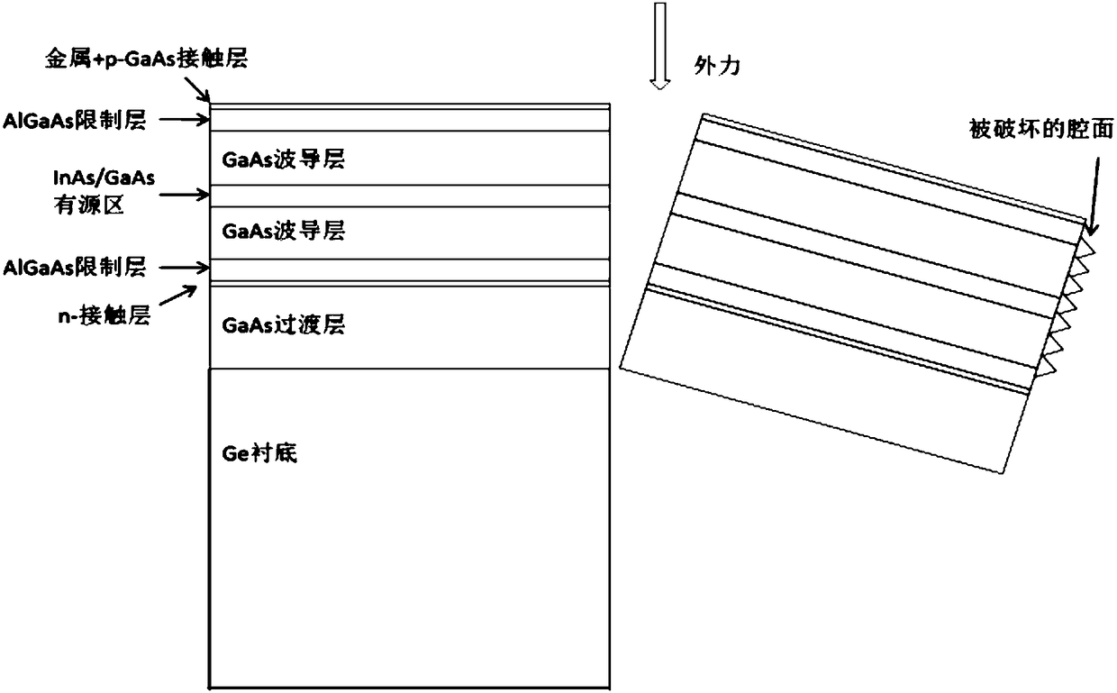
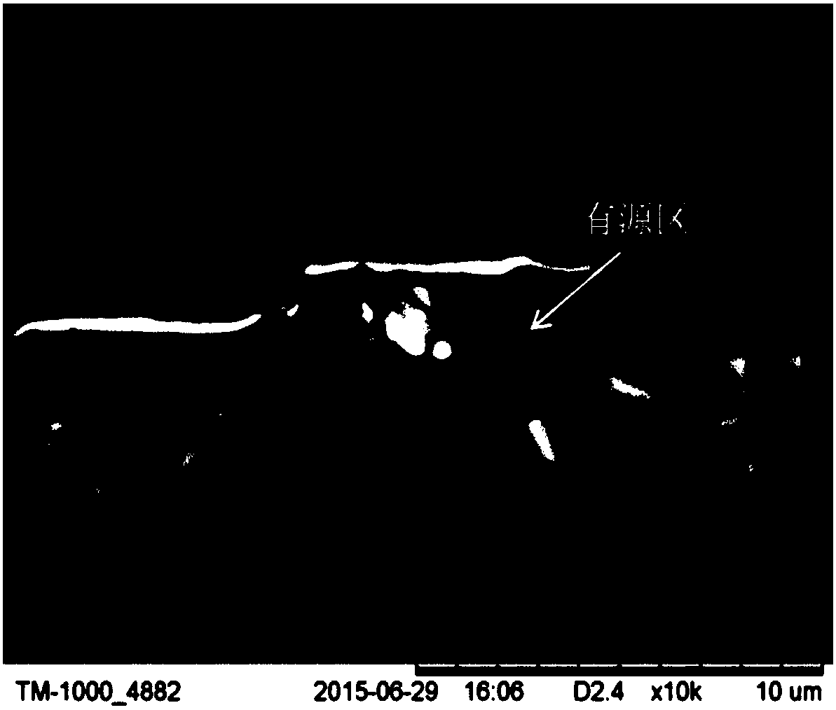
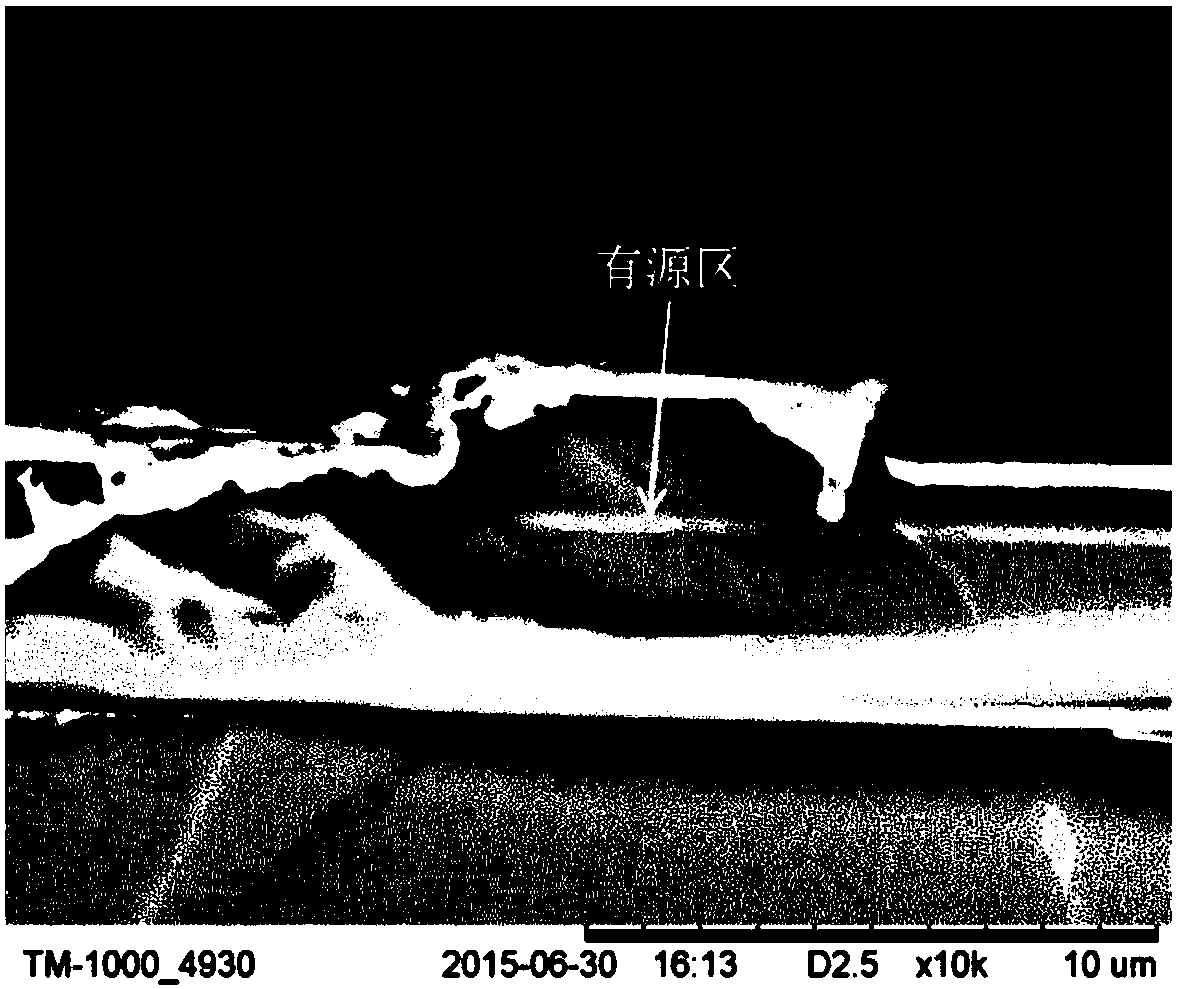
[0023] Cavity surface regeneration of Ge-based InAs / GaAs quantum dot edge-emitting lasers:

[0024] ①First, place the packaged laser on a heating platform with a temperature of 180°C, remove the wire immediately after the indium melts, and remove the laser from the heat sink. This process should always be carried out on the heating platform , and avoid the molten indium solution from sticking to the cavity surface of the laser.

[0025] ②Preparation of cantilever structure on laser cavity surface: using H 2 o 2 Corrosion the failed laser, the corrosion condition is 50 ℃ water bath heating for 8h, under this condition, the corrosion liquid hardly affects the InAs / GaAs laser structure, the selection ratio is about 30:1; that is, the corrosion rate of GaAs is Ge substrate The corrosion rate is less than 1 / 30. Therefore, by choosing a suitable etching time, the Ge substrate can be etched laterally without corroding the epitaxial structure of the laser on the substrate, thereby ...


PUM


Abstract

The invention relates to a regeneration method of an edge-emitting semiconductor laser cavity surface. The method comprises the steps as follows: (1) selective corrosion is carried out on an invalid edge-emitting semiconductor laser by a high-selection ratio corrosive agent and a cantilever structure is formed on damaged cavity surfaces of resonant cavities at two ends of the laser; and (2) external force is applied to the position, close to the cavity surface of the laser, at the outer side of the cantilever structure by a press pin, the damaged cavity surfaces are naturally cleaved and a new cavity surface is formed. The invalid laser due to a COD problem can restore most of work performance; and the service lifetime of the laser is effectively prolonged.

Description

technical field [0001] The invention belongs to the field of semiconductors, in particular to a method for regenerating cavity surfaces of edge-emitting semiconductor lasers. Background technique [0002] Silicon-based optoelectronic integrated circuit technology uses the existing VLSI technology to integrate silicon-based optoelectronic devices and circuits on the same chip. Since silicon materials have absolute advantages in integration, both integrated optoelectronic technology and relatively mature microelectronics Technology is booming, which prompts optoelectronic devices to continue to move towards system integration. Silicon-based monolithic integrated chips with the advantages of compact structure and low cost are an important development direction. Since silicon is an indirect bandgap semiconductor, it is difficult to directly use it as an effective light source. The development of silicon-based III-V compound semiconductor lasers is an effective solution. At pres...

Claims


Application Information

Patent Timeline
Patent Type & Authority Patents(China)
IPC IPC(8): H01S5/10
CPCH01S5/1082
Inventor 王亚楠李耀耀王庶民曹春芳
Owner SHANGHAI INST OF MICROSYSTEM & INFORMATION TECH CHINESE ACAD OF SCI
Why Eureka
Try Eureka