Wiring board

A technology of wiring substrates and insulating substrates, which is applied to the layout details of conductive patterns, printed circuits, electrical components, etc., can solve the problems of impedance mismatch, signal reflection, and inability to transmit high-frequency signals efficiently, and achieves a lower impedance. Effect

Active Publication Date: 2016-07-13
KYOCERA CORP
View PDF3 Cites 0 Cited by
  • Summary
  • Abstract
  • Description
  • Claims
  • Application Information

AI Technical Summary

Problems solved by technology

As a result, an impedance mismatch occurs between the external connection pad 39a for differential signals and the through-conductor 36a

Method used


Image

  • Wiring board
  • Wiring board
  • Wiring board

Examples


Example Embodiment

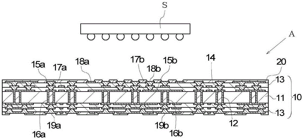
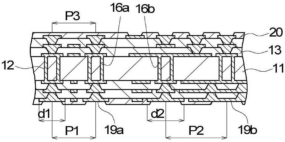
[0020] based on figure 1 as well as figure 2 A wiring board according to an embodiment will be described. figure 1 The illustrated wiring board A includes an insulating substrate 10 in which a plurality of insulating layers 13 having via holes 14 are laminated on the upper and lower surfaces of an insulating plate 11 having through holes 12 .

[0021] The insulating plate 11 is a member that becomes the core substrate of the wiring substrate A. As shown in FIG. The insulating plate 11 is formed of, for example, an electrical insulating material obtained by impregnating a thermosetting resin such as epoxy resin and bismaleimide triazine resin into a glass fabric woven into glass fiber bundles vertically and horizontally. owned. The thickness of the insulating plate 11 is about 0.3 to 1.5 mm. The diameter of the through hole 12 is about 0.1 to 0.3 mm.

[0022] Each insulating layer 13 laminated on the upper and lower surfaces of the insulating plate 11 is a reinforcing i...


PUM


Abstract

The wiring board in the present invention includes: an insulating board; external connection pads for a differential signal and external connection pads for grounding or a power supply formed on a lower surface of the insulating board; and a through-conductor formed in the insulating board. Each of the external connection pads is formed in a two-dimensional arrangement, a diameter and an arrangement pitch of the external connection pad for a differential signal are smaller than a diameter and an arrangement pitch of the external connection pad for grounding or a power supply, and an arrangement pitch of the through-conductor connected to the external connection pad for a differential signal is less than or equal to an arrangement pitch of the external connection pad for a differential signal.

Description

technical field [0001] The present invention relates to a wiring board for mounting semiconductor elements such as semiconductor integrated circuit elements. Background technique [0002] based on image 3 A conventional wiring board B for mounting a semiconductor element S' will be described. The wiring board B includes an insulating substrate 30 in which a plurality of insulating layers 33 having via holes 34 are stacked on upper and lower surfaces of an insulating plate 31 having through holes 32 . Such a wiring board is described in JP-A-2014-82393, for example. [0003] A plurality of conductors 35 a and 35 b are arranged on the surface and inside of the insulating substrate 30 . The conductor 35a is a conductor for differential signals. The conductor 35b is a conductor for grounding or power supply. Penetration conductors 36 a and 36 b are attached in the through hole 32 . The via conductor 36a is a via conductor for differential signals. The through conductor 36...

Claims


Application Information

Patent Timeline
IPC IPC(8): H05K1/11H01L23/498
CPCH01L23/49822H01L23/49838H05K1/111H05K2201/09427H05K1/0251H05K3/4602H05K3/4644H01L2224/16225H05K1/113H05K1/0245H05K1/0298
Inventor 中川芳洋
Owner KYOCERA CORP
Why Eureka
Try Eureka