Debugging method and system for programmable logic device

A programming logic and debugging system technology, applied in the debugging method and system field of programmable logic devices, can solve the problems that cannot meet the debugging requirements of FPGA technology, and achieve the effect of rich trigger condition configuration and simple use

Inactive Publication Date: 2016-07-20
SHENZHEN PANGO MICROSYST CO LTD
View PDF3 Cites 14 Cited by
  • Summary
  • Abstract
  • Description
  • Claims
  • Application Information

AI Technical Summary

Problems solved by technology

[0005] The invention provides a debugging method and system for programmable logic devices to solve the problem that

Method used


Image

  • Debugging method and system for programmable logic device
  • Debugging method and system for programmable logic device
  • Debugging method and system for programmable logic device

Examples


Example

[0033] First embodiment:

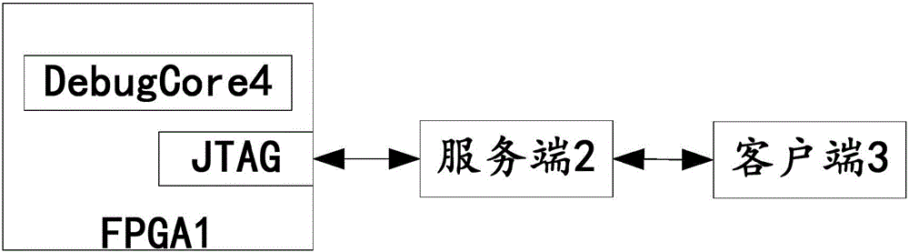
[0034] figure 1 It is a schematic structural diagram of the debugging system provided by the first embodiment of the present invention, which is represented by figure 1 It can be seen that in this embodiment, the debugging system provided by the present invention includes: a programmable logic device 1, a server 2, a client 3 and an enhanced logic analyzer core DebugCore4 embedded in a programmable logic device 1, wherein:

[0035] The client 3 is used to set the operating parameters of the enhanced logic analyzer core, and sends the bit stream file generated by compiling and compiling the operating parameters and the design to be tested to the server 2;

[0036] The server 2 is used to download the bit stream file to the programmable logic device 1;

[0037] The programmable logic device 1 is used to execute the design under test, and the enhanced logic analyzer core 4 collects and stores data according to the working parameters, and sends them to...

Example

[0044] Second embodiment:

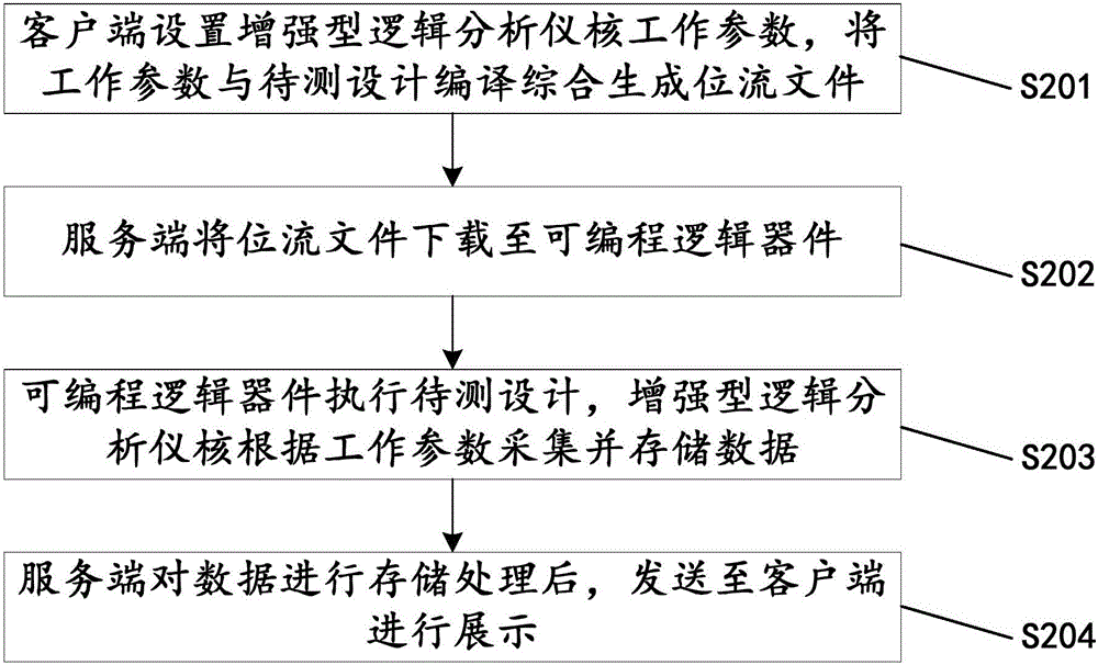
[0045] figure 2 The flow chart of the debugging method provided by the second embodiment of the present invention is composed of figure 2 It can be seen that in this embodiment, the debugging method provided by the present invention includes:

[0046] S201: The client sets the working parameters of the enhanced logic analyzer core, compiles and synthesizes the working parameters and the design under test to generate a bit stream file and sends it to the server;

[0047] S202: The server downloads the bit stream file to the programmable logic device;

[0048] S203: The programmable logic device executes the design under test, and the enhanced logic analyzer core collects and stores data according to the working parameters, and sends them to the server;

[0049] S204: After the server stores and processes the data, it sends it to the client for display.

[0050] In some embodiments, before the server downloads the bit stream file to the programm...

Example

[0056] Third embodiment:

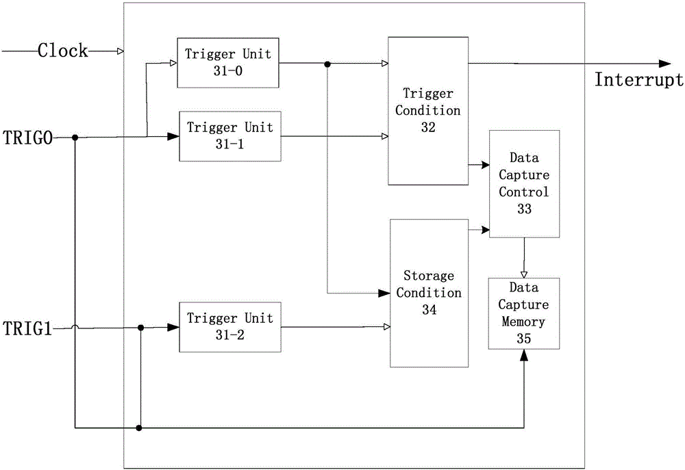
[0057] This embodiment provides an enhanced embedded logic analyzer based on PLD (programmablelogicdevice, programmable logic device), by inserting one or more logic analyzer cores in the FPGA design, the user can easily access the inside of the FPGA device All signals and nodes (including ports, wire nets and pins); by setting trigger conditions, the signals to be observed are triggered, data collected, stored, and displayed and observed on the client; used to solve the problem of ultra-high Density FPGA debugging is inconvenient. The embedded enhanced logic analyzer has the ability to support multiple DebugCores (enhanced logic analyzer cores) to sample data at the same time. When powering on and initializing, the configuration of grabbing signals and trigger conditions is more abundant and easy to use. Simple and other features, and has a powerful data analysis display function through the client.

[0058] In actual use, the embedded logic analyz...


PUM


Abstract

The invention provides a debugging method and system for a programmable logic device.The method comprises the steps that a client side sets working parameters of an enhanced type logic analyzer core, and compiles the working parameters and design to be detected to comprehensively generate a bitstream file to be sent to a service side; the service side downloads the bitstream file to the programmable logic device; the programmable logic device executes the design to be tested, and the enhanced type logic analyzer core collects and stores data according to the working parameters and sends the data to the service side.The service side stores and processes the data and then sends the data to the client side.By means of the debugging method and system, enhanced type logic analyzer core is embedded into the programmable logic device, data sampling output is carried out on the design to be tested through the enhanced type logic analyzer core, no external logic analyzer or oscilloscope needs to be adopted in the process, testing points do not need to be planned on a circuit board, and pin resources are not occupied.

Description

technical field [0001] The invention relates to the field of integrated circuit design, in particular to a debugging method and system for programmable logic devices. Background technique [0002] In the FPGA (Field Programmable Gate Array, Field Programmable Gate Array) design process, most of the time will be spent on debugging and troubleshooting, and equipment such as logic analyzers and oscilloscopes are the most important debugging tools. [0003] In the prior art, when using a logic analyzer and an oscilloscope for debugging, it is necessary to connect the probes to the signals to be tested on the circuit board, and then set the logic analyzer to capture the required signals for observation, analysis and debugging. When designing and verifying an ultra-high-density FPGA with this debugging method, it is difficult to connect to a circuit board made of a fine-pitch process, and it is difficult to lead out I / O pins, and it may even change the original state of the signal...

Claims


Application Information

Patent Timeline
IPC IPC(8): G06F17/50
CPCG06F30/34
Inventor 苏金欢陈燕生
Owner SHENZHEN PANGO MICROSYST CO LTD
Why Eureka
Try Eureka