Double-sided light emitting device for OLED display screen and preparation method

A double-sided light-emitting, display screen technology, applied in electrical components, electric solid-state devices, circuits, etc., can solve problems such as complex processes, and achieve the effects of simple process, improved color rendering index, and low production costs

Inactive Publication Date: 2016-07-20
BEIJING VISIONOX TECH
View PDF11 Cites 8 Cited by
  • Summary
  • Abstract
  • Description
  • Claims
  • Application Information

AI Technical Summary

Problems solved by technology

[0004] In view of this, the main purpose of the present invention is to provide a double-sided light-emitting device for OLED display screens, which has a thinner structure and can solve the technical problems of complex processes

Method used


Image

  • Double-sided light emitting device for OLED display screen and preparation method
  • Double-sided light emitting device for OLED display screen and preparation method

Examples


no. 1 example

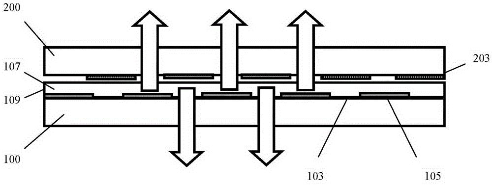
[0032] Please refer to figure 1 , the OLED display double-sided light-emitting device of the present invention includes a substrate 100, an anode layer, an organic light-emitting layer 109, a cathode layer 107, and an encapsulation cover 200 stacked in sequence, wherein the anode layer includes transparent Anode layer 103 and non-transparent anode layer 105 ; opaque positions and transparent positions arranged in a matrix form and complementary to the transparent anode layer 103 and non-transparent anode layer 105 are arranged inside the package cover 200 .

[0033] Preferably, the anode material is a material with high work function and light transmittance. As a specific example, the anode is a transparent conductive film of ITO with a high work function of 4.5eV-5.3eV, stable properties and light transmission.

[0034] Preferably, the opaque positions of the package cover 200 and the light-emitting areas on the substrate 100 using opaque metal as anodes are arranged in a sta...

no. 2 example

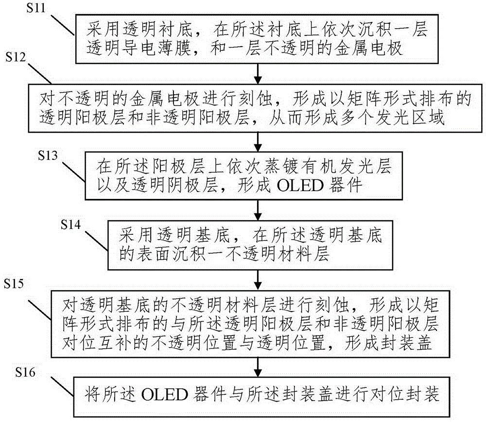
[0041] This embodiment is to provide a method for preparing an OLED display device that emits light on both sides, including: S11, using a transparent substrate, and sequentially depositing a layer of transparent conductive film and a layer of opaque metal electrodes on the substrate; S12, etching the opaque metal electrode to form a transparent anode layer and a non-transparent anode layer arranged in a matrix, thereby forming multiple light-emitting regions; S13, sequentially vapor-depositing an organic light-emitting layer and a transparent anode layer on the anode layer A cathode layer, forming an OLED device; S14, using a transparent substrate, depositing an opaque material layer on the surface of the transparent substrate; S15, etching the opaque material layer of the transparent substrate to form a matrix arranged in a matrix with the transparent The anode layer and the non-transparent anode layer align complementary opaque positions and transparent positions to form an ...


PUM


Abstract

The invention discloses a double-sided light emitting device for an OLED display screen and a preparation method. The device comprises a substrate, an anode layer, an organic light-emitting layer, a cathode layer and a packaging cover, which are sequentially stacked, wherein the anode layer comprises transparent anode layers and non-transparent anode layers, which are arranged in a matrix form; and non-transparent positions and transparent positions, which are arranged in the matrix form and are complementary with the transparent anode layers and the non-transparent anode layers in an aligned manner, are arranged at the inner side of the packaging cover. Compared with an existing scheme of adding two packaging covers after double-sided evaporation, the structure is relatively thin; the process is simple; and a high-precision mask plate is not needed in preparation, so that the double-sided light emitting device has the advantage of low cost.

Description

technical field [0001] The invention belongs to the technical field of organic light-emitting display, and in particular relates to a double-sided light-emitting device and a preparation method of an OLED display screen. Background technique [0002] OLED has the advantages of high contrast, wide viewing angle, low power consumption, and thinner volume. It is expected to become the next-generation flat-panel display technology after LCD. It is one of the most concerned technologies in flat-panel display technology. Generally speaking, organic light-emitting The display device includes a plurality of OLED pixel circuits arranged in a matrix, and each OLED pixel circuit includes an OLED device and a corresponding driving circuit. Organic light emitting display devices display images using organic light emitting diodes, and OLEDs generate light through recombination of electrons and holes. Organic light emitting display devices have the characteristics of high response speed a...

Claims


Application Information

Patent Timeline
Patent Type & Authority Applications(China)
IPC IPC(8): H01L27/32
Inventor 朱映光张国辉
Owner BEIJING VISIONOX TECH
Why Eureka
Try Eureka