Thin film transistor and preparation method thereof, array substrate, and display device

A technology of thin film transistors and substrate substrates, applied in the direction of transistors, semiconductor/solid-state device manufacturing, semiconductor devices, etc., can solve problems such as large leakage current, difficulty in forming PN structure, and performance degradation of LTPSTFT devices

Active Publication Date: 2016-07-20
BOE TECH GRP CO LTD
View PDF4 Cites 32 Cited by
  • Summary
  • Abstract
  • Description
  • Claims
  • Application Information

AI Technical Summary

Problems solved by technology

[0003] In the existing LTPSTFT device, when the TFT is in the off state, due to the influence of the parasitic capacitance of the TFT itself, a strong electric field is formed in the drain depletion region. Under the action of this electric fi

Method used


Image

  • Thin film transistor and preparation method thereof, array substrate, and display device
  • Thin film transistor and preparation method thereof, array substrate, and display device
  • Thin film transistor and preparation method thereof, array substrate, and display device

Examples


Embodiment Construction

[0047] The following will clearly and completely describe the technical solutions in the embodiments of the present invention with reference to the accompanying drawings in the embodiments of the present invention. Obviously, the described embodiments are only some, not all, embodiments of the present invention. Based on the embodiments of the present invention, all other embodiments obtained by persons of ordinary skill in the art without making creative efforts belong to the protection scope of the present invention.

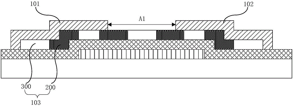
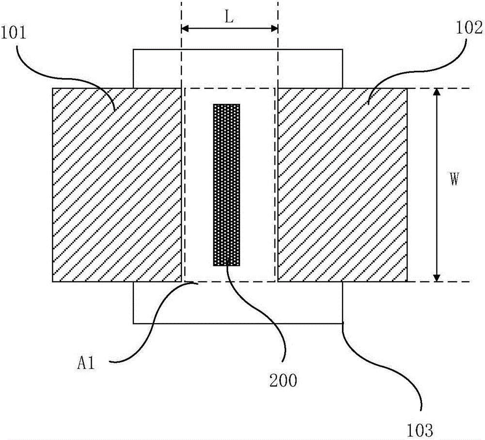
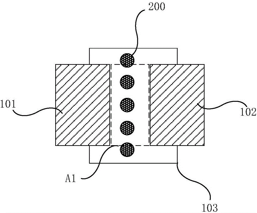
[0048] An embodiment of the present invention provides a thin film transistor, such as figure 1As shown, the thin film transistor includes a source 101, a drain 102, and a semiconductor active layer 103. The semiconductor active layer 103 is divided into an amorphous silicon portion 200 and a polysilicon portion 300. At least a part of the amorphous silicon portion 200 is located at the source 101. and the drain 102; wherein, the amorphous silicon portion 200 ...


PUM


Abstract

One embodiment of the invention provides a thin film transistor and a preparation method thereof, an array substrate, and a display device, and relates to the technical field of display, which can reduce leakage current of thin film transistors on the premise that the thin film transistor electron mobility is guaranteed. The thin film transistor comprises a source electrode, a drain electrode, and a semiconductor active layer, wherein the semiconductor active layer is divided into an amorphous silicon part and a polycrystalline silicon part; at least part of the amorphous silicon part is located between the source electrode and the drain electrode; the amorphous silicon part is mainly made of amorphous silicon and the polycrystalline silicon part is mainly made of polycrystalline silicon.

Description

technical field [0001] The invention relates to the field of display technology, in particular to a thin film transistor and a preparation method thereof, an array substrate, and a display device. Background technique [0002] With the development of liquid crystal display technology, the requirements for the electron mobility of the thin film transistor (ThinFilmTransistor, TFT) semiconductor layer are higher, and the low temperature polysilicon thin film transistor (LowTemperaturePoly-siliconThinFilmTransistor, LTPSTFT) came into being. It can be prepared under relatively low temperature conditions (below 600°C), has the advantages of flexible substrate selection and low preparation cost, so it has been widely used in various electronic displays including electronic products such as computers and mobile phones. [0003] In the existing LTPSTFT device, when the TFT is in the off state, due to the influence of the parasitic capacitance of the TFT itself, a strong electric fi...

Claims


Application Information

Patent Timeline
IPC IPC(8): H01L29/786H01L21/336
CPCH01L29/6675H01L29/78609H01L29/7866H01L29/78696
Inventor 何晓龙薛建设曹占锋孙雪菲张斌
Owner BOE TECH GRP CO LTD
Why Eureka
Try Eureka