
Thin-film transistor substrate, manufacturing method thereof and display panel

A technology of a thin film transistor and a manufacturing method, which is applied in the field of thin film transistor substrates, can solve problems such as light leakage and transmittance reduction, and achieve the effects of reducing light leakage, increasing resolution, and improving display effect.

Active Publication Date: 2016-07-27
HONG FU JIN PRECISION IND (SHENZHEN) CO LTD +1
View PDF4 Cites 1 Cited by
  • Summary
  • Abstract
  • Description
  • Claims
  • Application Information

AI Technical Summary

Problems solved by technology

[0003] Since the thin film transistor array substrate and the color filter substrate are manufactured independently and then aligned into a box together, there will be at least two thicknesses of the substrates. At the same time, there is an alignment deviation when the two substrates are aligned. It will lead to defects such as light leakage and lower transmittance; moreover, with the increase in the resolution of end products, when the resolution of small and medium-sized products is increased to 500ppi or even higher, it is difficult to make the contact on the color filter with the existing technology. The size of the hole can meet the requirements of less than 5um or even smaller

Method used


Image

  • Thin-film transistor substrate, manufacturing method thereof and display panel
  • Thin-film transistor substrate, manufacturing method thereof and display panel
  • Thin-film transistor substrate, manufacturing method thereof and display panel

Examples


Embodiment Construction

[0021] Please also see Figures 1 to 9 , which is a cross-sectional view of each step of the manufacturing method of the thin film transistor substrate 11 according to a preferred embodiment of the present invention. The method comprises the steps of:

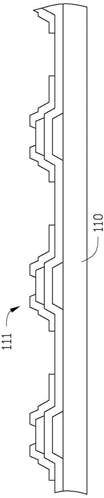
[0022] Step S01, such as figure 1 As shown, a first substrate 110 is provided, and a plurality of thin film transistors 111 are formed on the first substrate 110 .

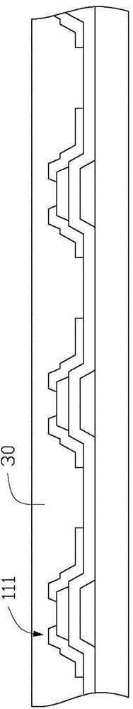
[0023] Step S02, such as figure 2 As shown, a first photoresist layer 30 is formed on the first substrate 110 and the thin film transistors 111 , and the first photoresist layer 30 covers a plurality of the thin film transistors 111 . In this embodiment, the first photoresist layer 30 is a positive photoresist.

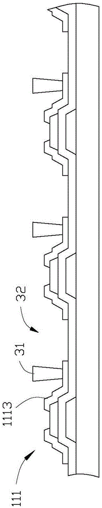
[0024] Step S03, such as image 3 As shown, the first photoresist layer 30 is patterned to form a spacer 31 at a position above the drain 1113 of the thin film transistor 111 . There are gaps 32 between adjacent spacers 31 . In this embodiment, th...


PUM

PropertyMeasurementUnit
Thicknessaaaaaaaaaa

Abstract

The invention provides a thin-film transistor substrate, a manufacturing method thereof and a display panel provided with the thin-film transistor substrate. The display panel includes a thin-film transistor substrate, an opposite substrate arranged opposite to the thin-film transistor substrate, and a liquid crystal layer sandwiched between the thin-film transistor substrate and the opposite substrate. According to the technical scheme of the display panel, a color filter layer is formed on the thin-film transistor substrate. Meanwhile, a positive photoresist and a negative photoresist are cooperatively used at the same time. In this way, the prepared color filter layer has small-size contact holes. Therefore, the thickness of the display panel is effectively reduced and the defects of light leakage, lower permeability and the like, caused by alignment deviation, are reduced. At the same time, the resolution of the display panel is increased and the display effect of the display panel is improved.

Description

technical field [0001] The invention relates to a thin film transistor substrate, its manufacturing method and a display panel with the thin film transistor substrate. Background technique [0002] Displays are now widely used in various display fields, such as households, public places, office places and personal electronic related products. To develop in a higher direction. At present, liquid crystal display devices have developed from Twisted Nematic (TN) liquid crystal displays with simple fabrication, low cost and small viewing angle to multi-dimensional electric field (Advanced SuperDimension Switch, AD-SDS, referred to as ADS) liquid crystal display devices, and based on The HADS type liquid crystal display device of the high aperture ratio that ADS mode proposes, no matter which kind of liquid crystal display device, the manufacture technology of its liquid crystal display panel all is to manufacture thin-film transistor array substrate and color filter substrate se...

Claims


Application Information

Patent Timeline
IPC IPC(8): H01L21/84H01L27/12G02F1/1362G02F1/1368
Inventor 吴美玲侯智元郑新安林洋钜
Owner HONG FU JIN PRECISION IND (SHENZHEN) CO LTD
Features
  • Generate Ideas
  • Intellectual Property
  • Life Sciences
  • Materials
  • Tech Scout
  • Unparalleled Data Quality
  • Higher Quality Content
  • 60% Fewer Hallucinations
Learn More