Display substrate, fabrication method thereof and display device

A technology for a display substrate and a manufacturing method, which is applied to semiconductor devices, electrical components, circuits, etc., can solve problems such as poor lines, glass debris easily crushed or scratched data line wiring patterns, etc., to avoid bad lines.

Active Publication Date: 2016-07-27
BOE TECH GRP CO LTD +1
View PDF3 Cites 7 Cited by
  • Summary
  • Abstract
  • Description
  • Claims
  • Application Information

AI Technical Summary

Problems solved by technology

And because the passivation layer set on the data line pattern in the peripheral metal line is relatively thin, the glass debri

Method used


Image

  • Display substrate, fabrication method thereof and display device
  • Display substrate, fabrication method thereof and display device
  • Display substrate, fabrication method thereof and display device

Examples


Embodiment Construction

[0040] In order for those skilled in the art to better understand the technical solution of the present invention, the display substrate provided by the present invention, its manufacturing method, and the display device are described in detail below with reference to the accompanying drawings.

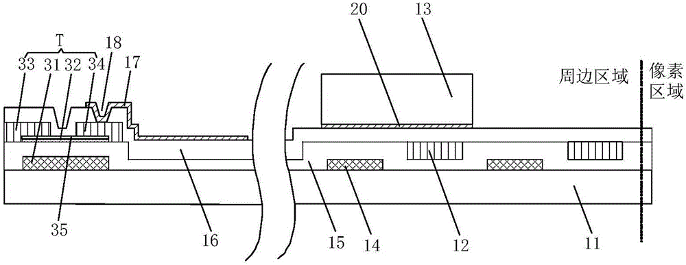
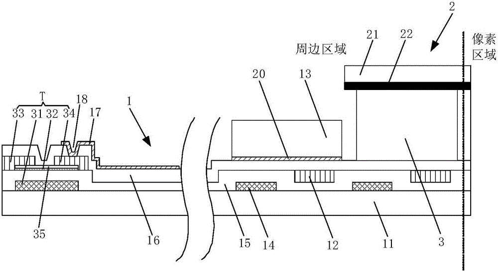
[0041] figure 1 A schematic structural diagram of a display substrate provided in Embodiment 1 of the present invention, as shown in figure 1 As shown in , a display area and a peripheral area located around the display area are formed on the display substrate. The display substrate includes a first base substrate 11 and a first wiring pattern 12 above the first base substrate 11, the first wiring pattern 12 is located in the peripheral area, and a photoresist is arranged above the first wiring pattern 12 Keep figure 13.

[0042] In this embodiment, a second wiring pattern 14 is also arranged above the first base substrate 11, the second wiring pattern 14 is located in the periphera...


PUM

PropertyMeasurementUnit
Thicknessaaaaaaaaaa

Abstract

The invention discloses a display substrate, a fabrication method thereof and a display device. A display region and a surrounding region arranged around the display region are formed on the display substrate, the display substrate comprises a first substrate and a first wiring pattern, the first wiring pattern is arranged above the first substrate and is arranged in the surrounding region, and a photoresist reservation pattern is arranged above the first wring pattern. In the display device, the fabrication method thereof and the technical scheme of the display device, provided by the invention, the photoresist reservation pattern is arranged above the first wiring pattern in the surrounding region, broken glass generated by cutting and damage to the wring pattern by press or scratch of other foreign objects are avoided, and thus, unfavorable line generation is prevented.

Description

technical field [0001] The invention relates to the field of display technology, in particular to a display substrate, a manufacturing method thereof, and a display device. Background technique [0002] Thin film transistor liquid crystal display (TFT-LCD) occupies a dominant position in the current flat panel display market due to its small size, low power consumption, and no radiation. Among them, the Twisted Nematic (abbreviation: TN) liquid crystal display device has become the most widely used entry-level liquid crystal display device due to its low production cost, and has short response time and high brightness. The TN type liquid crystal display device mainly controls the deflection of the liquid crystal through the vertical electric field formed between the pixel electrode (PixelITO) of the array substrate and the common electrode (CommonITO) of the color filter substrate to realize the liquid crystal display. Currently, among the mainstream low-end liquid crystal ...

Claims


Application Information

Patent Timeline
IPC IPC(8): H01L27/12
CPCH01L27/1214H01L27/1288
Inventor 卢彦春冯伟
Owner BOE TECH GRP CO LTD
Why Eureka
Try Eureka