Thin optical system, image acquisition device and electronic device

An optical system, thin technology, applied in the field of imaging device and electronic device, thin optical system, can solve the problems of large volume, reduce the portability of electronic device, reduce the volume of biometric system, etc.

Active Publication Date: 2016-08-03
LARGAN PRECISION
View PDF13 Cites 27 Cited by
  • Summary
  • Abstract
  • Description
  • Claims
  • Application Information

AI Technical Summary

Problems solved by technology

[0002] At present, most of the biometric identification systems used in mobile devices on the market use the principle of capacitance. Although it has the benefit of reducing the size of the biometric identification system, the complex circuit structure leads to high manufacturing costs, often resulting in high unit prices and difficult universal
[0003] Although there are traditional bio...

Method used


Image

  • Thin optical system, image acquisition device and electronic device
  • Thin optical system, image acquisition device and electronic device
  • Thin optical system, image acquisition device and electronic device

Examples


no. 1 example

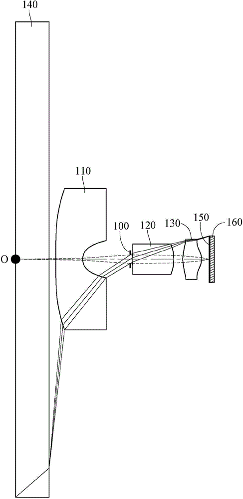
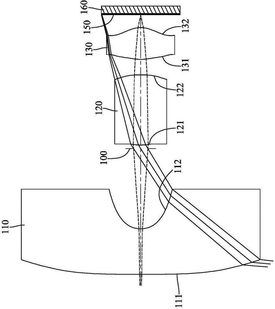
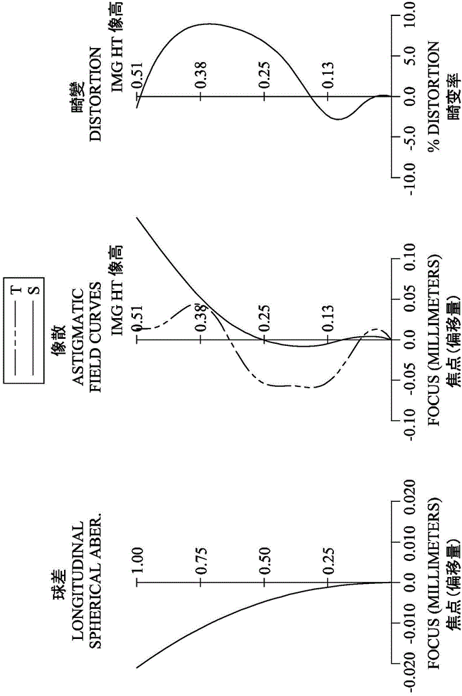
[0128] Please refer to Figure 1A , 1 Figure B and figure 2 ,in Figure 1A A schematic diagram of an imaging device according to a first embodiment of the present invention is shown, Figure 1B draw Figure 1A The partially enlarged schematic diagram of figure 2 From left to right are the spherical aberration, astigmatism and distortion curves of the first embodiment. Depend on Figure 1A and Figure 1B It can be seen that the image capturing device includes a thin optical system (not another number) and an electronic photosensitive element 160 . The thin optical system sequentially includes a flat plate element 140 , a first lens 110 , an aperture 100 , a second lens 120 , a third lens 130 and an imaging surface 150 from the object side to the image side. Wherein, the electronic photosensitive element 160 is disposed on the imaging surface 150 . There are three lenses (110-130) with refractive power in the thin optical system.

[0129] The first lens 110 has negative r...

no. 2 example

[0163] Please refer to Figure 3A , Figure 3B and Figure 4 ,in Figure 3A A schematic diagram of an imaging device according to a second embodiment of the present invention is shown, Figure 3B draw Figure 3A The partially enlarged schematic diagram of Figure 4 From left to right are the spherical aberration, astigmatism and distortion curves of the second embodiment. Depend on Figure 3A and Figure 3B It can be seen that the image capturing device includes a thin optical system (not another number) and an electronic photosensitive element 260 . The thin optical system sequentially includes a flat plate element 240 , a first lens 210 , an aperture 200 , a second lens 220 , a third lens 230 and an imaging surface 250 from the object side to the image side. Wherein, the electronic photosensitive element 260 is disposed on the imaging surface 250 . There are three lenses (210-230) with refractive power in the thin optical system.

[0164] The first lens 210 has neg...

no. 3 example

[0176] Please refer to Figure 5A , Figure 5B and Figure 6 ,in Figure 5A A schematic diagram of an imaging device according to a third embodiment of the present invention is shown, Figure 5B draw Figure 5A The partially enlarged schematic diagram of Figure 6 From left to right are the spherical aberration, astigmatism and distortion curves of the third embodiment. Depend on Figure 5A and Figure 5B It can be seen that the image capturing device includes a thin optical system (not otherwise labeled) and an electronic photosensitive element 360 . The thin optical system sequentially includes a flat plate element 340 , a first lens 310 , an aperture 300 , a second lens 320 , a third lens 330 and an imaging surface 350 from the object side to the image side. Wherein, the electronic photosensitive element 360 is disposed on the imaging surface 350 . There are three lenses (310-330) with refractive power in the thin optical system.

[0177] The first lens 310 has ne...


PUM

PropertyMeasurementUnit
Wavelengthaaaaaaaaaa

Abstract

The invention discloses a thin optical system, an image acquisition device and an electronic device. The thin optical system comprises a first lens, a second lens and a third lens with refractive power sequentially from an object side to an image side, wherein the first lens has negative refractive power, and the image side surface is a concave surface near an optical axis; the second lens has refractive power, at least one surface is an aspheric surface, and the second lens is made of plastic; the third lens has positive refractive power, at least one surface is an aspheric surface, and the third lens is made of plastic. Three lenses with refractive power exist in the thin optical system. The thin optical system further comprises an aperture arranged between the first lens and the second lens. The first lens, the second lens and the third lens have no mutual relative movement on the optical axis. When a specific condition is met, the thin optical system can be designed to be retrofocus, thereby enhancing telecentric effects. The invention also discloses an image acquisition device provided with the above thin optical system and the electronic device provided with the image acquisition device.

Description

technical field [0001] The invention relates to a thin optical system, an image pickup device and an electronic device, in particular to a thin optical system and an image pickup device suitable for the electronic device. Background technique [0002] At present, most of the biometric identification systems used in mobile devices on the market use the principle of capacitance. Although it has the benefit of reducing the size of the biometric identification system, the complex circuit structure leads to high manufacturing costs, often resulting in high unit prices and difficult universal. [0003] Although there are traditional biometric identification systems using the principle of optical imaging, such as fingerprint identification, vein identification, etc., the traditional biometric identification system has the problem of being too large, which makes it difficult for the electronic device equipped with the identification system to be miniaturized and thinned, thereby red...

Claims


Application Information

Patent Timeline
IPC IPC(8): G02B13/18G02B13/00G02B3/02
Inventor 陈冠铭黄歆璇
Owner LARGAN PRECISION
Why Eureka
Try Eureka