Piezoelectric thin film element, piezoelectric actuator, piezoelectric sensor, hard-disk drive and ink jet printer device

A technology of piezoelectric actuators and piezoelectric films, applied in piezoelectric devices/electrostrictive devices, piezoelectric/electrostrictive/magnetostrictive devices, electrical components, etc., can solve the oxygen deficiency pressure of piezoelectric films Electrical characteristics, influence and other issues, to achieve the effect of reducing leakage current density, improving piezoelectric characteristics, and improving performance

Active Publication Date: 2016-08-03
TDK CORPARATION
View PDF5 Cites 4 Cited by
  • Summary
  • Abstract
  • Description
  • Claims
  • Application Information

AI Technical Summary

Problems solved by technology

[0004] The piezoelectric thin film constituting the piezoelectric thin film element is formed by a film-forming method called sputtering or chemical vapor deposition (CVD), but oxygen defects occur in the piezoelectric thin film during the film-forming process and these structural defects will affect the Its piezoelectric properties have a great influence on

Method used


Image

  • Piezoelectric thin film element, piezoelectric actuator, piezoelectric sensor, hard-disk drive and ink jet printer device
  • Piezoelectric thin film element, piezoelectric actuator, piezoelectric sensor, hard-disk drive and ink jet printer device
  • Piezoelectric thin film element, piezoelectric actuator, piezoelectric sensor, hard-disk drive and ink jet printer device

Examples


no. 1 Embodiment approach

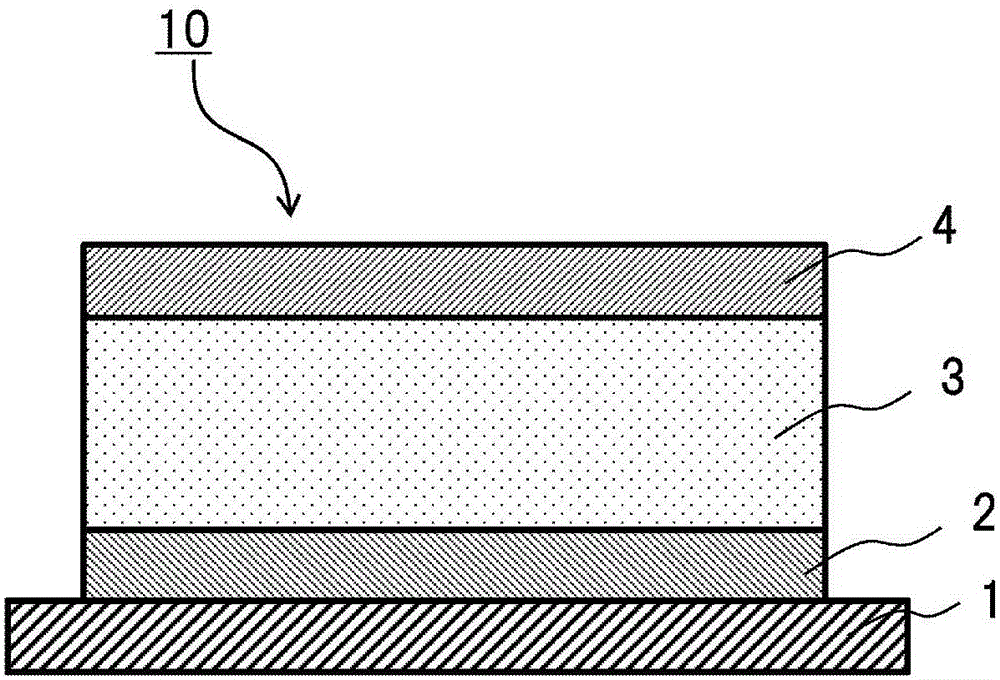
[0050] exist figure 1 The structure of the piezoelectric thin film element 10 of this embodiment is shown in .

[0051] As the substrate 1, a single crystal silicon substrate, a silicon-on-insulator (SOI) substrate, a quartz glass substrate, a compound semiconductor substrate made of GaAs or the like, a sapphire substrate, a metal substrate made of stainless steel or the like, a MgO substrate, SrTiO 3 As the substrate, a single crystal silicon substrate is particularly preferable from the viewpoint of substrate cost and process handling. The thickness of the substrate 1 is usually 10 to 1000 μm.

[0052]A lower electrode layer 2 is formed on a substrate 1 . The lower electrode layer 2 is formed by simultaneous film formation of Pt and the oxide material contained therein, and the film formation conditions in the binary sputtering of the Pt target and the oxide material target or the binary vapor deposition of two materials Thus, fine adjustment of the oxide content in the l...

no. 2 Embodiment approach

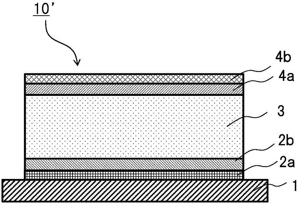
[0060] In the case of improving the piezoelectric characteristics of the piezoelectric thin film element and further improving leakage current suppression, the following configurations can be adopted. exist figure 2 The structure of the piezoelectric thin film element 10' of this embodiment is shown in .

[0061] As the substrate 1, a single crystal silicon substrate, a silicon-on-insulator (SOI) substrate, a quartz glass substrate, a compound semiconductor substrate made of GaAs or the like, a sapphire substrate, a metal substrate made of stainless steel or the like, a MgO substrate, SrTiO 3 As the substrate, a single crystal silicon substrate is particularly preferable from the viewpoint of substrate cost and process handling. The thickness of the substrate 1 is usually 10 to 1000 μm.

[0062] The first lower electrode layer 2 a is formed on the substrate 1 . The first lower electrode layer 2a is formed by simultaneous film formation of Pt and the contained oxide materia...

no. 3 Embodiment approach

[0071] When reducing the resistance value of the piezoelectric thin film element with priority, the following aspects are also applicable. exist figure 2 The structure of the piezoelectric thin film element 10' of this embodiment is shown in .

[0072] As the substrate 1, a single crystal silicon substrate, a silicon-on-insulator (SOI) substrate, a quartz glass substrate, a compound semiconductor substrate made of GaAs or the like, a sapphire substrate, a metal substrate made of stainless steel or the like, a MgO substrate, SrTiO 3 As the substrate, a single crystal silicon substrate is particularly preferable from the viewpoint of substrate cost and process handling. The thickness of the substrate 1 is usually 10 to 1000 μm.

[0073] The first lower electrode layer 2 a is formed on the substrate 1 . The material of the first lower electrode layer 2a is Pt that does not contain oxide materials, and the formation method is sputtering or vapor deposition. The film thickness...


PUM

PropertyMeasurementUnit
thicknessaaaaaaaaaa
thicknessaaaaaaaaaa

Abstract

The present invention aims to compensate the oxygen vacancy of a piezoelectric thin film forming a piezoelectric thin film element, further improve the piezoelectric characteristic and further reduce the leakage current density. The piezoelectric thin film element provided by the invention is characterized by having a pair of electrode layers and a piezoelectric thin film sandwiched between the pair of electrode layers, wherein the pair of electrode layers are composed of platinum (Pt), oxide particles are contained in at least one of the electrode layers, and the oxide particles are oxide particles of at least one element constituting the piezoelectric thin film or oxide particles of Pt.

Description

technical field [0001] The present invention relates to a piezoelectric thin film element using a piezoelectric thin film; a piezoelectric actuator and a piezoelectric sensor using the piezoelectric thin film element; and a hard disk drive and an inkjet printing apparatus including the piezoelectric actuator. Background technique [0002] In recent years, the practical use of piezoelectric elements using piezoelectric thin films instead of bulk piezoelectric materials has progressed. Examples include a gyro sensor, a pressure sensor, a pulse wave sensor, a shock sensor, and a microphone, which are piezoelectric sensors utilizing the piezoelectric effect that converts force applied to a piezoelectric film into a voltage. In addition, examples of piezoelectric actuators utilizing the inverse piezoelectric effect in which the piezoelectric film deforms when a voltage is applied to the piezoelectric film include magnetic head assemblies for hard disk drives, inkjet print heads, ...

Claims


Application Information

Patent Timeline
Patent Type & Authority Applications(China)
IPC IPC(8): H01L41/047H01L41/113B41J2/01G11B5/35
CPCB41J2/01G11B5/35H10N30/878H10N30/302H10N30/877H10N30/1051H10N30/2047H10N30/8542H10N30/20G11B5/483B41J2/14233
Inventor 佐久间仁志太田龙
Owner TDK CORPARATION
Why Eureka
Try Eureka