Chip structure with bonding wire

A chip structure and chip technology, applied in semiconductor/solid-state device parts, semiconductor devices, electrical components, etc., can solve the problems of damaged joint strength, large stress concentration, copper wire is not easy to deform, etc., and achieve good joint strength effect

Inactive Publication Date: 2016-08-10
IND TECH RES INST
View PDF4 Cites 1 Cited by
  • Summary
  • Abstract
  • Description
  • Claims
  • Application Information

AI Technical Summary

Problems solved by technology

However, the interface between the copper bonding wire and the aluminum pad on the chip is prone to chemical reactions to generate intermetallic compounds under the high-temperature working environment of high-power automotive power modules. Holes between them destroy the bonding strength
In addition, the hardness of the copper bonding wire is higher than that of the aluminum pad, which means that the copper bonding wire is less likely to be deformed during the bonding process. Therefore, it is necessary to increase the bonding force during bonding to make the copper bonding wire produce enough deformation to achieve good performance. However, this may cause greater stress concentration and damage the lower hardness aluminum pads or cause damage to the chip under the aluminum pads

Method used


Image

  • Chip structure with bonding wire
  • Chip structure with bonding wire

Examples


Embodiment Construction

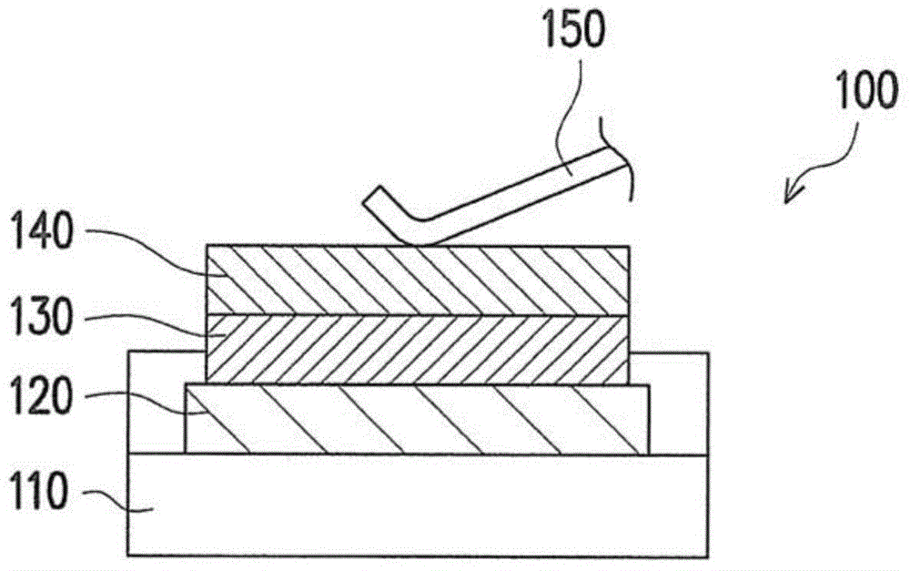
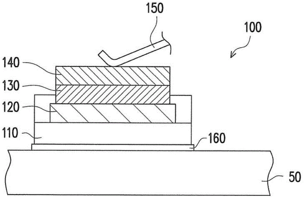
[0025] figure 1 It is a schematic diagram of the chip structure of an embodiment of the present invention. Please refer to figure 1 , the chip structure 100 of this embodiment includes a chip 110 , a first metal layer 130 , a second metal layer 140 and bonding wires 150 . The pads 120 are disposed on the chip 110 , and the first metal layer 130 is disposed on the chip 110 . The material of the first metal layer 130 is, for example, nickel or nickel alloy. The second metal layer 140 is disposed on the first metal layer 130 , and the material of the second metal layer 140 is, for example, copper, copper alloy, aluminum, aluminum alloy, palladium or palladium alloy. The bonding wire 150 is connected to the second metal layer 140 by, for example, a wedge bond manufacturing process. The material of the bonding wire 150 is, for example, copper or a copper alloy, and the wire diameter of the bonding wire 150 is, for example, larger than 102 microns to be suitable for high Power mo...


PUM


Abstract

The invention discloses a chip structure with a bonding wire. The chip structure comprises a chip, a first metal layer, a second metal layer and a bonding wire. The first metal layer is disposed on the chip, and the material of the first metal layer includes nickel or nickel alloy. The second metal layer is disposed on the first metal layer, and the material of the second metal layer includes copper, copper alloy, aluminum, aluminum alloy, palladium or palladium alloy. The wire is connected to the second metal layer, and the material of the bonding wire comprises copper or copper alloy.

Description

technical field [0001] The present invention relates to a chip structure, and in particular to a chip structure with bonding wires. Background technique [0002] Due to the crisis of oil depletion, automobile energy-saving technology is the most important goal of the development of human civilization at this stage. As the population structure is concentrated in cities, people’s daily commuting time by car is gradually increasing, and the aging of the population makes the driving time longer. Therefore, personal electric vehicles that focus on vehicle body space, safety and energy saving are gradually developing. The industry and Research units are actively investing in the research and development of this related technology. [0003] Wire bonding is one of the key technologies for automotive power modules. In the past, aluminum bonding wires were mostly used for wire bonding of automotive power modules. However, as the power of automotive power modules has increased signif...

Claims


Application Information

Patent Timeline
Patent Type & Authority Applications(China)
IPC IPC(8): H01L23/488
CPCH01L24/45H01L2224/45124H01L2224/45147H01L24/05H01L2224/4847H01L2224/45015H01L24/32H01L24/73H01L2224/02166H01L2224/05082H01L2224/05155H01L2224/05624H01L2224/32225H01L2224/73265H01L2924/00014H01L2924/13055H01L2924/13091H01L24/48H01L2224/04042H01L2224/05124H01L2224/05147H01L2224/05647H01L2924/00015H01L2924/2076H01L2224/29099H01L24/08H01L2224/05582H01L2224/05655H01L2224/05664H01L2224/48455H01L2224/4801
Inventor 林育民林柏丞张景尧
Owner IND TECH RES INST
Why Eureka
Try Eureka