LED Packaging Structure And Method For Manufacturing The Same
A technology of LED packaging and packaging structure, which is applied in the direction of semiconductor devices, electrical components, circuits, etc., can solve the problems of reduced reliability of LED chip packaging structure, low yield, and pollution of the mold space on the side of the chip.
- Summary
- Abstract
- Description
- Claims
- Application Information
AI Technical Summary
Problems solved by technology
Method used
Image

Examples
Embodiment Construction
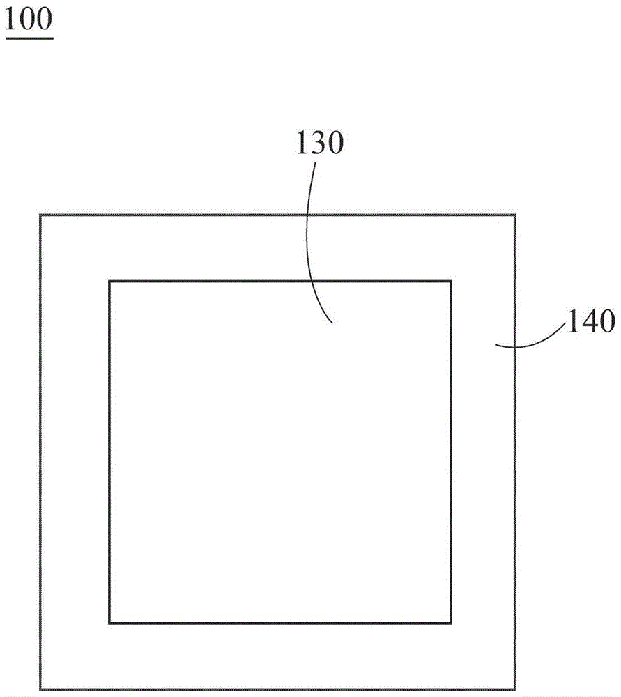
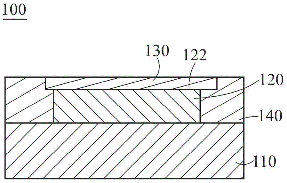
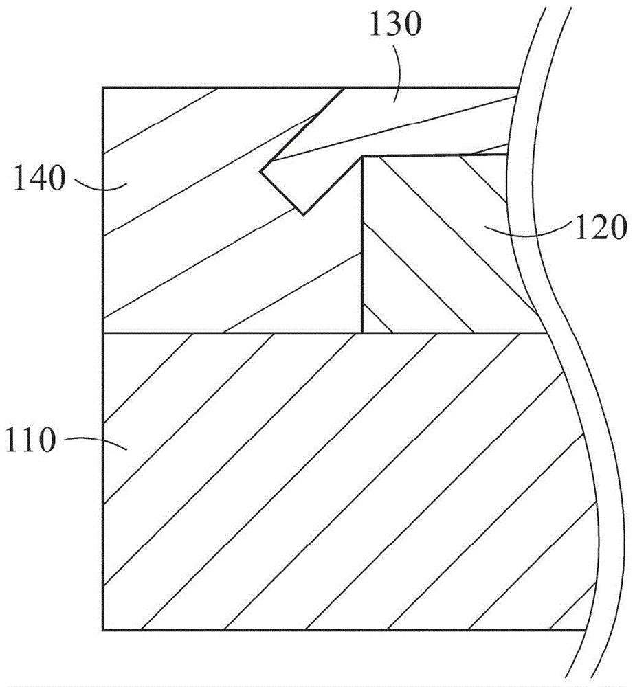
[0067] An LED packaging structure described in the present invention uses an LED chip (such as blue LED or ultraviolet UV-LED) to emit a light beam (such as blue light or ultraviolet light), and then the light beam excites the fluorescent sheet or fluorescent colloid. To produce white light, and further provide a uniform light emitting area.
[0068] First please refer to figure 1 and Figure 2A , which are respectively a top view and a cross-sectional view of the LED packaging structure 100 according to the first embodiment of the present invention. As shown in the figure, the LED packaging structure 100 includes a substrate 110 , an LED chip 120 , a fluorescent sheet 130 and a first glue 140 . Wherein, the LED chip 120 is arranged on the substrate 110, and the LED chip 120 has an upper surface 122; the fluorescent sheet 130 has a first area, and the fluorescent sheet 130 is attached to the upper surface 122 of the LED chip 120; the first colloid 140 It is disposed on the ...
PUM
 Abstract
Description
Claims
Application Information
 - R&D
- Intellectual Property
- Life Sciences
- Materials
- Tech Scout
- Unparalleled Data Quality
- Higher Quality Content
- 60% Fewer Hallucinations
Browse by: Latest US Patents, China's latest patents, Technical Efficacy Thesaurus, Application Domain, Technology Topic, Popular Technical Reports.
© 2025 PatSnap. All rights reserved.Legal|Privacy policy|Modern Slavery Act Transparency Statement|Sitemap|About US| Contact US: help@patsnap.com