Preparation method of ceramic substrate for high-power LED packaging

A technology for LED packaging and ceramic substrates, which is applied to the preparation of metal circuits on the surface of ceramic substrates and the field of preparation of ceramic substrates, can solve the problems of poor surface flatness, high technical requirements, complex processes, etc. The effect of improving the bonding strength and reducing the peeling problem

Inactive Publication Date: 2012-05-02
江苏景邦照明科技有限公司
View PDF3 Cites 38 Cited by
  • Summary
  • Abstract
  • Description
  • Claims
  • Application Information

AI Technical Summary

Problems solved by technology

It has high bonding strength, but poor surface flat...

Method used


Image

  • Preparation method of ceramic substrate for high-power LED packaging
  • Preparation method of ceramic substrate for high-power LED packaging
  • Preparation method of ceramic substrate for high-power LED packaging

Examples


Embodiment 1

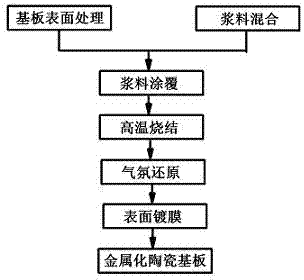
[0038] Step 1: Dissolve 5 grams of vinyl chloride resin in 40 grams of ethylene glycol ether at a constant temperature of 70°C until completely dissolved, and filter to obtain an organic vehicle; dissolve 3 grams of γ-aminopropyltriethoxysilane in ethanol Diluted into a solution with a volume ratio of 5%, and then added 50 grams of cuprous oxide particles with a particle size of 10 μm, stirred evenly, and dried at 70 ° C. Added the ground and crushed particles and 2 grams of polyethylene wax to the above organic In the carrier, stir evenly to obtain a slurry;

[0039] Step 2: After the alumina ceramics are mechanically polished, they are ultrasonically cleaned in ethanol and dried; then, the slurry prepared in step 1 is coated on the ceramic substrate by screen printing to form a circuit pattern, and dried at 300°C;

[0040] Step 3: Put the coated ceramic substrate prepared in step 2 into an electric furnace, heat it in the air to 1150° C. 2 +H 2 heated to 800°C for 1 hour i...

Embodiment 2

[0044] Step 1: Dissolve 1.5 grams of polyester resin in 5 grams of ethylene glycol ether and 10 grams of terpineol at a constant temperature of 90°C until completely dissolved, and filter to obtain an organic vehicle; 0.1 grams of vinyl tris(β- Methoxyethoxy) silane was diluted in ethanol to a solution with a volume ratio of 0.1%, and then 80 grams of cuprous oxide particles with a particle size of 0.1 μm were added, stirred evenly, dried at 60 ° C, and ground and pulverized Particles and 0.1 g of polyamide wax are added to the above-mentioned organic carrier, and stirred evenly to obtain a slurry;

[0045] Step 2: After the SiC ceramic is mechanically polished, it is ultrasonically cleaned in ethanol and dried; then the slurry prepared in step 1 is coated on the ceramic substrate by spraying and masking to form a circuit pattern, and the circuit pattern is formed at 100 ° C drying;

[0046] Step 3: Put the coated ceramic substrate prepared in Step 2 into an electric furnace,...

Embodiment 3

[0050] Step 1: Dissolve 3 grams of polyester resin in 35 grams of terpineol at a constant temperature of 80°C until completely dissolved, and filter to obtain an organic vehicle; Dilute titanium in ethanol to a solution with a volume ratio of 1%, and then add 60 grams of cuprous oxide particles with a particle size of 50 μm, stir evenly, and dry at 65 ° C. Grind and pulverize the particles, 1 gram of oleic acid amide wax Adding to the above-mentioned organic carrier, stirring evenly to obtain a slurry;

[0051] Step 2: Chemically polish the aluminum nitride ceramics, ultrasonically clean them in ethanol, and dry them; then use spin coating and photolithography to coat the slurry prepared in step 1 on the ceramic substrate to form a circuit pattern. Drying at 200°C;

[0052] Step 3: Put the coated ceramic substrate prepared in Step 2 into an electric furnace, heat it in the air to 1100° C. for 2 hours, and then cool it with the furnace. Then put the prepared substrate into a ...


PUM

PropertyMeasurementUnit
Particle sizeaaaaaaaaaa

Abstract

The invention provides a preparation method of a ceramic substrate for high-power LED packaging, comprising the following steps of: preparing for the surface-processed ceramic substrate, covering the ceramic substrate with prepared cuprous oxide slurry, forming a circuit diagram, drying, sintering, reducing and plating a film to prepare ceramic substrate with a smooth and compact metal surface. With the combination of a thick film technology and a bonded copper principle on the surface of the ceramic substrate, metallization is realized without coating equipment and a complex technology required by a thin preparation technology and a special technology for direct bonded copper. In addition, with the combination of a direct bonded copper principle, the bonding strength of the metal layer and ceramic is raised and the spalling problem caused by thermal shock is minimized. According to the invention, the technology is simple; large-scale equipment is not required; raw materials are low-priced; the yield is high; metal patterning is convenient; surface fineness is high; and the copper layer thickness on the surface of the substrate is especially controllable so as to make the operation of a power electronic device more stable.

Description

technical field [0001] The invention relates to a preparation method of a ceramic substrate with excellent performance, in particular to a preparation method of a metal circuit on the surface of the ceramic substrate. The ceramic substrate prepared according to the above preparation method can be used for packaging high-power LEDs and belongs to the technical field of electronic packaging. [0002] Background technique [0003] With the development of electronic technology, electronic products are developing in the direction of high integration, small size, high power and high speed, which makes the heat generation of electronic components more and more large, so higher requirements are put forward for the heat dissipation of electronic device packaging Require. [0004] Compared with traditional lighting, high-power LEDs have attracted much attention due to their advantages such as high luminous efficiency, long life, and small size. Nearly 70% of the dissipated energy of...

Claims


Application Information

Patent Timeline
IPC IPC(8): C04B41/88
Inventor 宋秀峰周鸣刘乃涛侯君凯陆英艳
Owner 江苏景邦照明科技有限公司
Why Eureka
Try Eureka