Nano graphical and ultrawide-band electromagnetic property measuring system

A technology of electromagnetic characteristics and nano-patterns, applied in the fields of electromagnetic field characteristics, radio-frequency circuit testing, and measuring devices, can solve the problems of difficult patterning process, cumbersome processing and measurement process, prolonging the testing time of nano-materials and devices, etc., to achieve Extensive application fields and market demands, rapid and efficient testing and research results

Active Publication Date: 2013-01-30
INST OF PHYSICS - CHINESE ACAD OF SCI +1
View PDF9 Cites 6 Cited by
  • Summary
  • Abstract
  • Description
  • Claims
  • Application Information

AI Technical Summary

Problems solved by technology

Due to the difficulty of the patterning process at the nanoscale, the long preparation cycle, and the cumbersome processing and measurement processes, it not only increases the manufacturing cost, but also greatly prolongs the testing time of nanomaterials and devices, and the success rate and yield rate are also significantly affected. Impact
In addition, although the current electron beam exposure system integrates a probe arm with nanoscale positioning function, it cannot complete precise nanopositioning in a large range of 1 inch or more, and can only achieve small (several micron) positioning. ) to complete the positioning and connection of the probe and the sample

Method used


Image

  • Nano graphical and ultrawide-band electromagnetic property measuring system
  • Nano graphical and ultrawide-band electromagnetic property measuring system
  • Nano graphical and ultrawide-band electromagnetic property measuring system

Examples


Embodiment Construction

[0085] Below in conjunction with accompanying drawing, structural principle and working principle of the present invention are specifically described:

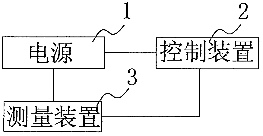
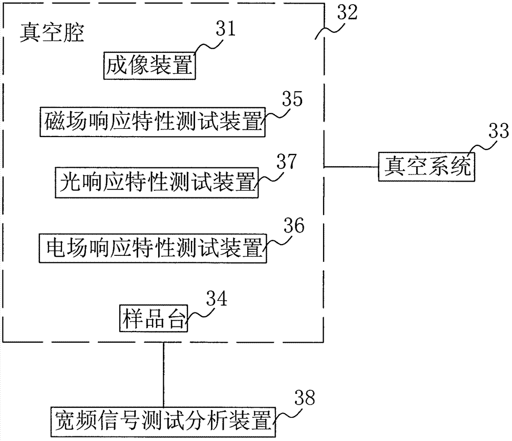
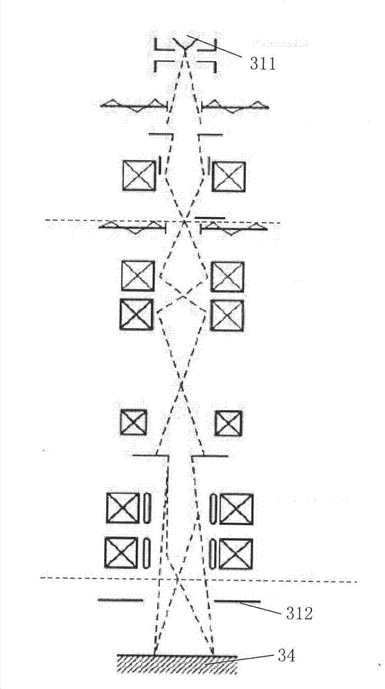
[0086] The invention introduces the measuring magnetic field to the sample stage with the function of SEM imaging or EBL patterning, so as to realize the test of the magnetic field response characteristic of the tested nanometer material or device. see figure 1 , figure 2 and image 3 , figure 1 It is a structural block diagram of the present invention, figure 2 It is a structural block diagram of a measuring device according to an embodiment of the present invention, image 3 It is a working principle diagram of the imaging device of the present invention. The nano-patterning and ultra-broadband electromagnetic characteristic measurement system of the present invention includes a power supply 1, a control device 2 and a measurement device 3, the control device 2 is connected to the measurement device 3, the control dev...


PUM


Abstract

A nano graphical and ultrawide-band electromagnetic property measuring system comprises a power source, a control device and a measuring device. The control device and the measuring device are connected and respectively connected with the power source. The measuring device comprises an imaging device with an SEM (scanning electron microscope) imaging or EBL (electron beam lithography) graphical function, a vacuum cavity, a vacuum system, a sample platform and a magnetic field response property testing device, wherein the vacuum system is connected with the vacuum cavity; the imaging device, the sample platform and the magnetic field response property testing device are arranged in the vacuum cavity; and the imaging device and the magnetic field response property testing device are arranged in correspondence to the sample platform. The nano graphical and ultrawide-band electromagnetic property measuring system can quickly efficiently test and research nano materials and devices and display samples thereof and has wide application range and high market demands.

Description

technical field [0001] The invention relates to a detection device for nanomaterials and devices, especially a magnetic field application based on an electron beam exposure system / electron beam pattern generation system, high-frequency electromagnetic signal generation, introduction, transmission and measurement, and nano-positioning in a large range Nanopatterning and ultra-wideband electromagnetic characteristic measurement system. Background technique [0002] With the development of nano-processing and detection technology, nano-materials and devices have been widely used in many fields including electronics, magnetism, chemistry, and biology. Research on nanomaterials and devices has become one of the core issues in condensed matter physics, modern information technology and industrial production. Since 1988, the rapid development of spintronics is gradually bringing information science into an era of extremely high-density magnetic storage (T-bit / inch2) including nano...

Claims


Application Information

Patent Timeline
Patent Type & Authority Applications(China)
IPC IPC(8): G01B15/04G01R29/08
CPCH01J37/26H01J2237/28G01B15/04G01R29/08G01R31/2822G01R31/315H01J37/3174H01J2237/24564H01L22/12
Inventor 韩秀峰马勤礼于国强刘厚方余天周向前艾金虎孙晓玉
Owner INST OF PHYSICS - CHINESE ACAD OF SCI
Why Eureka
Try Eureka