Preparation method of patterned metal layer

A patterning, metal layer technology, applied in semiconductor/solid-state device manufacturing, electrical components, circuits, etc., can solve the problems of unclean metal removal, increased peeling difficulty, and inability to achieve peeling effect.

Active Publication Date: 2018-08-10
TSINGHUA UNIV
View PDF4 Cites 5 Cited by
  • Summary
  • Abstract
  • Description
  • Claims
  • Application Information

AI Technical Summary

Problems solved by technology

Therefore, during the metal deposition process, metal particles will be deposited on the slope, and the photoresist will be completely covered by the metal. When the photoresist is removed, the stripping solution will hardly penetrate the photoresist and cannot react with the photoresist. , resulti...

Method used


Image

  • Preparation method of patterned metal layer
  • Preparation method of patterned metal layer
  • Preparation method of patterned metal layer

Examples


preparation example Construction

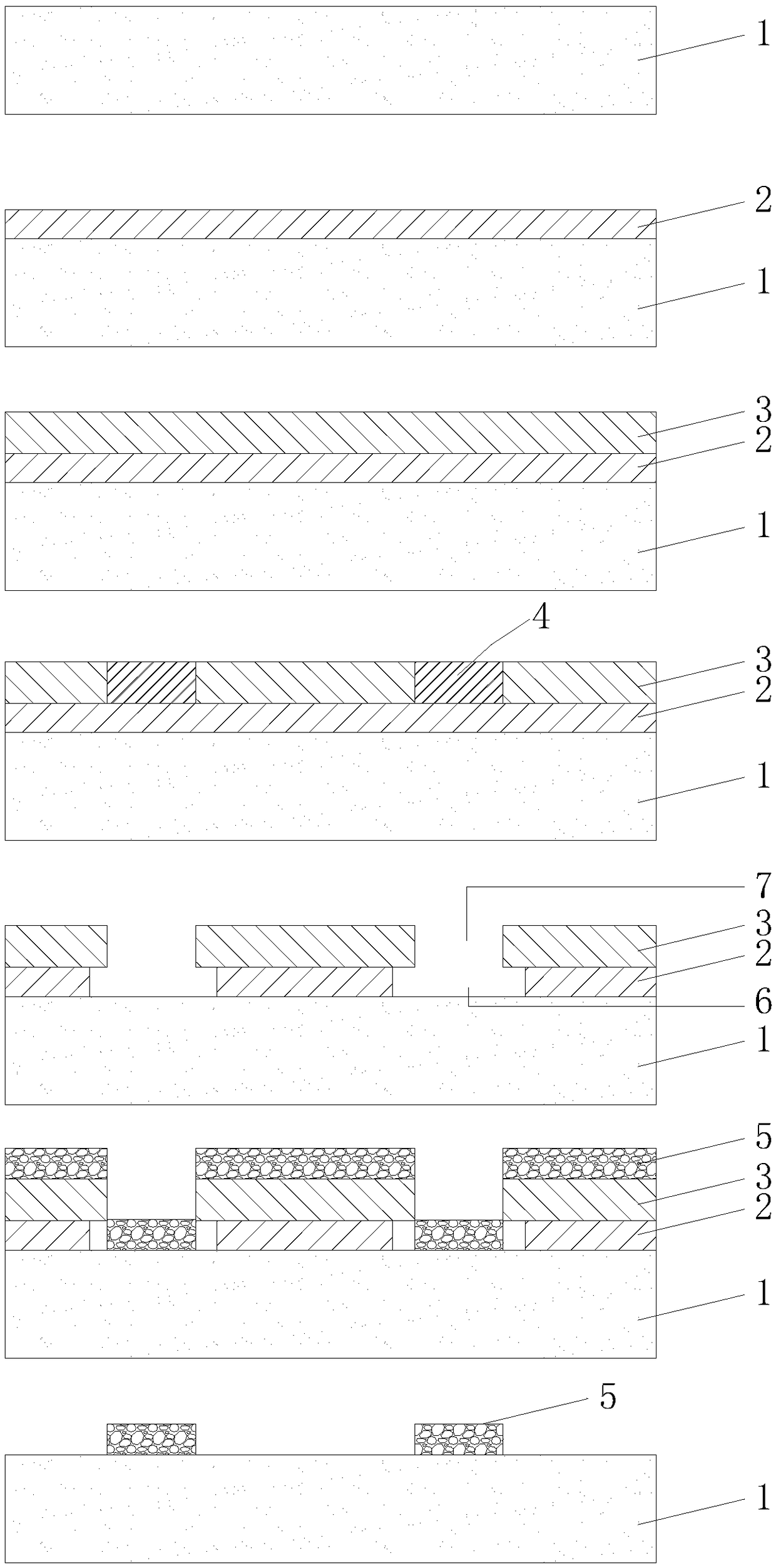
[0017] The preparation method of the graphic metal layer provided by the present invention will be further described below.

[0018] The invention provides a method for preparing a patterned metal layer, the preparation method comprising:

[0019] Provide a base, and sequentially form primer and photoresist on the base;

[0020] exposing the substrate with the primer and the photoresist and placing it in a developing solution for simultaneous patterning, wherein in the developing solution, the dissolution rate of the primer is greater than that of the exposed photoresist ;

[0021] Depositing a metal layer on the substrate with patterned primer and photoresist;

[0022] peeling off the underlayer glue and the photoresist to obtain a patterned metal layer.

[0023] The material of the bottom layer glue is LOR glue, and the photoresist is positive photoresist. Described LOR glue is a kind of non-photosensitive water-soluble macromolecule polymer, and chemical change can not ...

Embodiment 1

[0038] refer to figure 2 The process flow chart, using silicon wafers as the substrate 1, first clean the silicon wafers with RCA standard cleaning solution and dry them: when cleaning, first wash the silicon wafers in a volume ratio of 4:1 2 SO 4 with H 2 o 2 Wash in 5 min, rinse in deionized water after cleaning, and then put in NH with a volume ratio of 1:1:5 4 OH / H 2 o 2 Wash in a solution of deionized water for 5 minutes, rinse in deionized water after cleaning, and then put in HCl / H with a volume ratio of 1:1:4 2 o 2 Wash in a solution of deionized water for 5 minutes, rinse in deionized water after cleaning, then put in HF with a concentration of 2% for 30 seconds, and rinse in deionized water after cleaning. After cleaning, the silicon wafers were put into a spin dryer and dried at a speed of 2000r / min for 5min.

[0039] Use LOR-5B photoresist as the primer 2 and spread it evenly on the silicon wafer twice, with a thickness of 0.7 μm each time and a total thic...

Embodiment 2

[0049] refer to figure 2 The process flow chart, using silicon wafers as the substrate 1, first clean the silicon wafers with RCA standard cleaning solution and dry them: when cleaning, first wash the silicon wafers in a volume ratio of 4:1 2 SO 4 with H 2 o 2 Wash in 5 min, rinse in deionized water after cleaning, and then put in NH with a volume ratio of 1:1:5 4 OH / H 2 o 2 Wash in a solution of deionized water for 5 minutes, rinse in deionized water after cleaning, and then put in HCl / H with a volume ratio of 1:1:4 2 o 2 Wash in a solution of deionized water for 5 minutes, rinse in deionized water after cleaning, then put in HF with a concentration of 2% for 30 seconds, and rinse in deionized water after cleaning. After cleaning, the silicon wafers were put into a spin dryer and dried at a speed of 2000r / min for 5min.

[0050] Use LOR-5B photoresist as the primer 2 and spread it evenly on the silicon wafer twice, with a thickness of 0.5 μm each time and a total thic...


PUM

PropertyMeasurementUnit
Thicknessaaaaaaaaaa
Thicknessaaaaaaaaaa
Thicknessaaaaaaaaaa

Abstract

The invention relates to a preparation method of a patterned metal layer. The method comprises that a substrate is provided, and bottom glue and photoresist are formed on the substrate successively; the substrate with the bottom glue and photoresist are exposed and placed in a developing solvent for patterning the bottom glue and the photoresist at the same time, and in the developing solution, the dissolving speed of the bottom glue is greater than that of the exposed photoresist; a metal layer is deposited on the substrate with the patterned bottom glue and photoresist; and the bottom glue and photoresist are peeled to obtain the patterned metal layer. According to the preparation method, the bottom glue and photoresist are patterned in the developing solvent at the same time, formed patterns of the bottom glue and photoresist are wide in the upper and narrow in the lower, the metal layer is not deposited on the sidewall on the bottom glue, and metal connection is not formed. Thus, in the peeling process, a peeling solution can enter the bottom glue easily and dissolve the bottom glue and photoresist rapidly, the metal layer is peeled from the photoresist with a better peeling effect, and the needed patterned metal layer is obtained.

Description

technical field [0001] The invention relates to the field of semiconductor integrated circuits, in particular to a method for preparing a patterned metal layer. Background technique [0002] With the continuous improvement of micro-electro-mechanical systems and integrated circuit processing technology, the product technology used in it is also constantly developing, which has higher requirements for the lift-off process in the photolithography process. [0003] The photolithography process is one of the most frequently used and most critical technologies in the entire process. In essence, photolithography is a patterning process: when the photoresist is exposed to light of a specific wavelength, its chemical structure changes. Causes the photoresist to dissolve in a specific solution. The metal lift-off process is an important photolithography process and an important means of metal patterning. [0004] In the lift-off process, it is necessary to make a photoresist mask w...

Claims


Application Information

Patent Timeline
IPC IPC(8): H01L21/027
CPCH01L21/027
Inventor 阮勇尤政孙伟杨宋志强
Owner TSINGHUA UNIV
Why Eureka
Try Eureka