Preparation method for PCB plate with step trough

A PCB board and stepped groove technology, which is applied in the manufacturing of printed circuits, the formation of electrical connection of printed components, electrical components, etc., can solve the problems of patch processing, the inability to pattern the stepped grooves, and the protection of green oil, so as to reduce the volume. Effect

Active Publication Date: 2011-02-16
SHENNAN CIRCUITS
View PDF1 Cites 7 Cited by
  • Summary
  • Abstract
  • Description
  • Claims
  • Application Information

AI Technical Summary

Problems solved by technology

[0008] The technical problem to be solved by the present invention is to provide a method for preparing a PCB board with stepped grooves, so as to solve the problems that the stepped grooves of the PCB board in the prior art cannot be patterned, green oil protection, patch processing, etc.

Method used


Image

  • Preparation method for PCB plate with step trough
  • Preparation method for PCB plate with step trough

Examples


Embodiment Construction

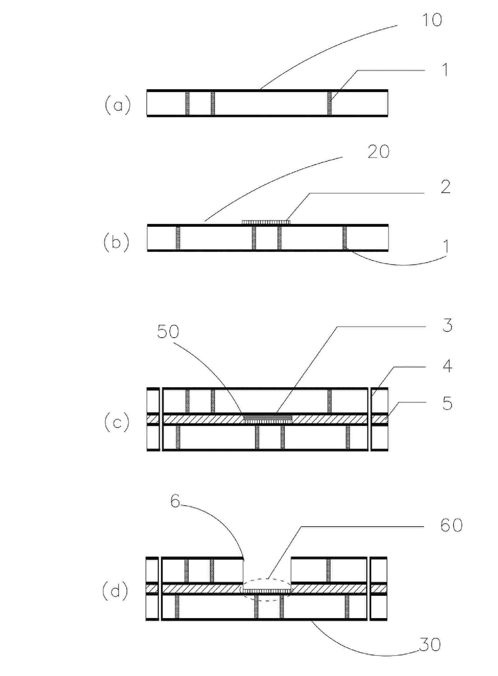
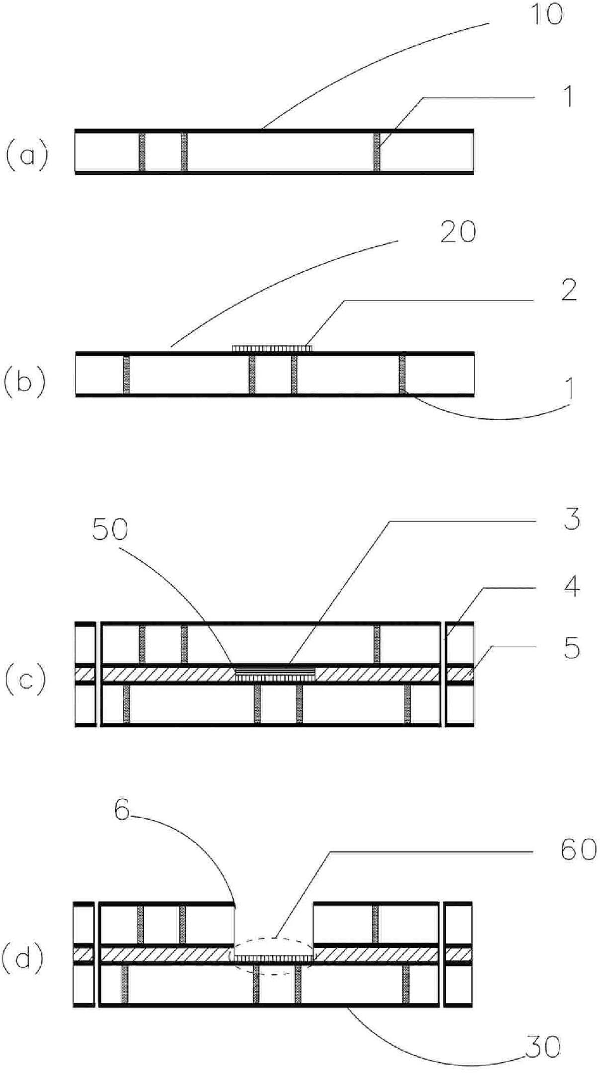
[0027] Please also refer to figure 1 , the present invention mainly utilizes the double pressing method to make the PCB board 30 with the stepped groove 6, which mainly includes the following steps: preparing the daughter boards 10 and 20, and making positioning holes (not shown) on the edge of the board; and preparing the mother board 30.

[0028] Please also refer to figure 1 (a), the sub-board 10 is a patterned laminated structure with through holes 1 drilled thereon, and a circuit (not shown) is formed in the sub-board 10 . The fabrication method of sub-board A mainly includes: inner layer fabrication, lamination, drilling, de-drilling, copper sinking, electroplating, plug hole, micro-etching, external drawing (outer layer image formation), and external etching (outer layer image etching) ) and other process steps. The sub-board 10 can be prepared by using the method for preparing a PCB board in the prior art. The inner layer fabrication includes forming circuits on ea...


PUM


Abstract

The invention relates to a preparation method for a PCB plate with a step trough, which comprises the following steps: a sub-plate one and a sub-plate two are prepared and compressed to prepare a motherboard, wherein the sub-plate one is formed by laminating and compressing an inner layer, the sub-plate two forms a green oil protective layer on a position to be formed with the step trough after laminating and compressing an inner layer. Steps for preparing the motherboard are as follows: a gasket is put on the green oil protective layer of the sub-plate two; the sub-plate one is laminated on the sub-plate two; dielectric layers are added between the two sub-plates and the periphery of the gasket and the green oil protective layer; the laminated sub-plates are compressed to form a motherboard; the motherboard is drilled with a through hole, is plated with copper and electroplated; and finally the motherboard is milled with a trough till reaching the position of the gasket; the excess PCB is taken out with the gasket to form the step trough. The invention adopts a secondary compression method, is simple, convenient and reliable, can form a pattern and the green oil protective layer at the bottom of the step trough, and further can paste and install electronic devices.

Description

technical field [0001] The invention relates to the manufacture of printed circuit boards, in particular to a preparation method of a PCB board with stepped grooves. Background technique [0002] At present, PCB boards with stepped groove design are mainly processed by one-time pressing, such as Chinese Patent Application No. CN200810142379.4, which mainly includes the following steps: providing an inner core board; providing a prepreg, and the prepreg is corresponding to the inner core board. Place the two prepregs on both sides of the inner core board; place the corresponding silica gel sheets in the stepped grooves of the prepregs; set steel sheets on the outside of the two prepregs, and press them together by a pressing machine, the prepregs flow glue, Forming; take out the silicone sheet in the stepped groove to form a stepped groove. In the processing method of the stepped PCB board of the invention, the silica gel sheet is filled in the stepped groove of the prepreg ...

Claims


Application Information

Patent Timeline
Patent Type & Authority Patents(China)
IPC IPC(8): H05K3/00H05K3/40
Inventor 李俊王彩霞陈于春
Owner SHENNAN CIRCUITS
Why Eureka
Try Eureka