
Electromagnetic wave shielding structure

A shielding structure and electromagnetic wave technology, applied in the direction of magnetic/electric field shielding, partial shielding, circuits, etc., can solve problems such as EMI leakage, performance degradation, degradation, etc., and achieve the effect of preventing EMI leakage and minimizing faults

Active Publication Date: 2019-11-01
LG INNOTEK CO LTD
View PDF6 Cites 0 Cited by
  • Summary
  • Abstract
  • Description
  • Claims
  • Application Information

AI Technical Summary

Problems solved by technology

[0002] Recently, with the integration of components and acceleration of processing speeds in electronic products, the performance of each component has been maximized, but there have been problems in that malfunctions, performance degradation, and degradation due to electromagnetic interference between adjacent components have occurred
[0004] However, in the case of metal members, there is a problem that the target device should be widely covered and adjacent devices as well as devices irrelevant to the corresponding performance should be covered, and the height of the metal member, the material of the metal member should be considered according to electronic components Thickness etc.
In addition, since it is difficult to completely perform shielding against electromagnetic interference, EMI leakage frequently occurs on the surface of the printed circuit board on which electronic components are mounted and on the portion coupled with the above-mentioned metal member

Method used


Image

  • Electromagnetic wave shielding structure
  • Electromagnetic wave shielding structure
  • Electromagnetic wave shielding structure

Examples


Embodiment Construction

[0017] The configuration and operation according to the present invention will be described in detail below with reference to the accompanying drawings. In the following description of the present invention, the same elements denote the same reference numerals regardless of symbols, and thus descriptions thereof will not be repeated. Although these terms, such as first, second, etc., may be used to describe various elements, these elements should not be limited to the above terms. The above terms are only used to distinguish one component from another.

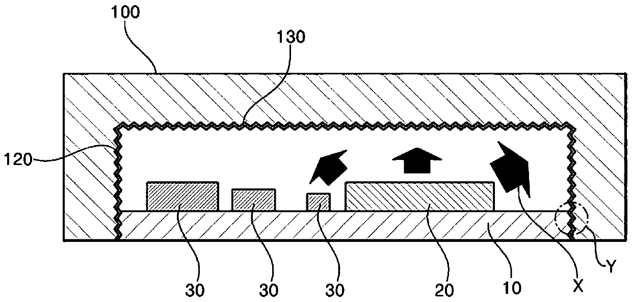
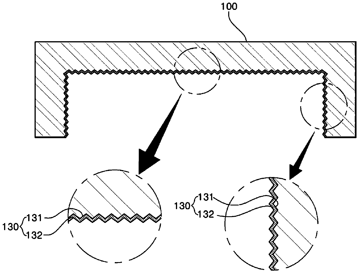
[0018] figure 1 is a schematic view of a package applying an electromagnetic wave shielding structure according to an embodiment of the present invention, and figure 2 yes figure 1 An enlarged schematic view of the electromagnetic shielding structure in .

[0019] see figure 1 and figure 2 , the electromagnetic wave shielding structure according to an embodiment of the present invention may include: an electromagnetic ...


PUM

PropertyMeasurementUnit
surface roughnessaaaaaaaaaa
thicknessaaaaaaaaaa

Abstract

The present invention relates to a structure capable of effectively shielding electromagnetic waves of electronic components. The electromagnetic wave shielding structure can fundamentally prevent electromagnetic interference (EMI) leakage and effectively shield electromagnetic waves of various electronic devices by forming a functional layer for shielding electromagnetic waves therein.

Description

technical field [0001] The present invention relates to a structure capable of effectively shielding electromagnetic waves of electronic components. Background technique [0002] Recently, with the integration of components and the acceleration of processing speeds in electronic products, the performance of each component is maximized, but there are problems in that malfunctions, performance degradation, and degradation due to electromagnetic interference between adjacent components occur. [0003] Electromagnetic interference (EMI) shielding is implemented on functionally classified unit devices by using metal members to prevent electromagnetic interference between adjacent electronic components and improve performance. [0004] However, in the case of metal members, there is a problem that the target device should be widely covered and also adjacent devices and devices irrelevant to the corresponding performance should be covered, and the height of the metal member, the ma...

Claims


Application Information

Patent Timeline
Patent Type & Authority Patents(China)
IPC IPC(8): H05K9/00
CPCH05K9/0024H05K9/003C25D5/12C23C18/1653C23C18/38H01L2924/1815H01L2924/3025H05K9/0088H05K9/0045
Inventor 玄淳莹裵硕尹兄权容栽李亨仪
Owner LG INNOTEK CO LTD
Learn More