GaN-based III-V compound semiconductor LED (light emitting diode) epitaxial wafer and production method thereof

A technology for LED epitaxial wafers and growth methods, which is applied in semiconductor devices, electrical components, circuits, etc., can solve problems such as the decline of optoelectronic properties such as the antistatic ability of LED chips, the easy formation of defects in the epitaxial layer, and the impact on the yield of chip products. Improve the internal quantum efficiency, enhance the antistatic ability, and improve the effect of compound efficiency

Active Publication Date: 2015-03-11
XIANGNENG HUALEI OPTOELECTRONICS
View PDF7 Cites 19 Cited by
  • Summary
  • Abstract
  • Description
  • Claims
  • Application Information

AI Technical Summary

Problems solved by technology

The substrates for growing GaN epitaxial layers with this structure often include SiC, Si, sapphire and other substrates. GaN epitaxial layers are grown heterogeneously on these substrates. Due to the large lattice adaptation, the epitaxial layers are easy to form defects and introduce Stress, crystal quality decline, lead to decline in photoelectric performance of LED chips such as antistatic ability, electrostatic failure has become a thorny problem affecting the yield of chip products

Method used


Image

  • GaN-based III-V compound semiconductor LED (light emitting diode) epitaxial wafer and production method thereof
  • GaN-based III-V compound semiconductor LED (light emitting diode) epitaxial wafer and production method thereof
  • GaN-based III-V compound semiconductor LED (light emitting diode) epitaxial wafer and production method thereof

Examples


Embodiment 1

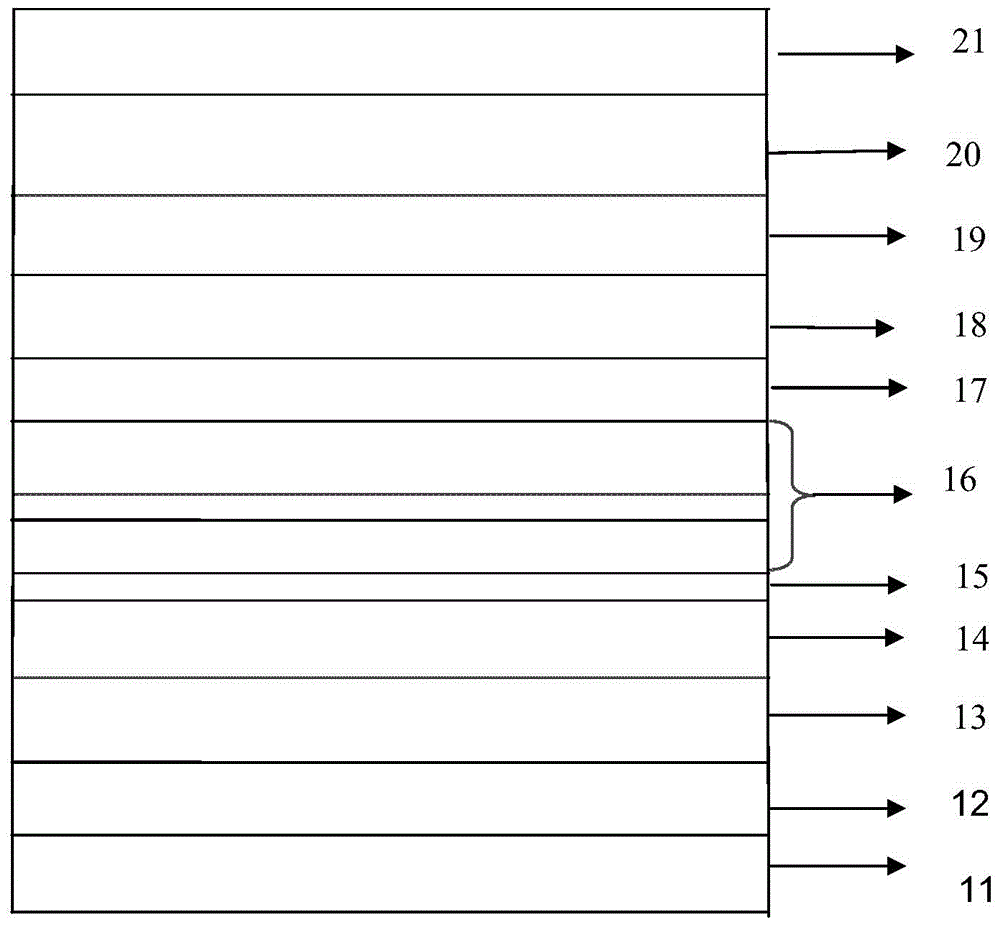
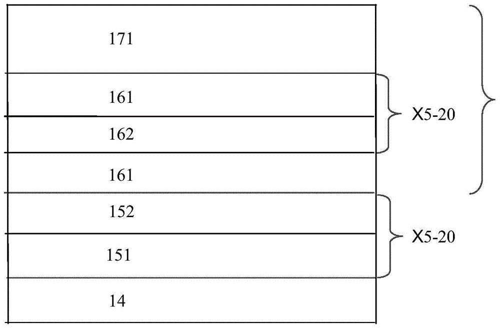
[0040] Please refer to figure 2 , the GaN-based Group III-V compound semiconductor LED epitaxial wafer of the present invention, its structure from bottom to top is: substrate 11, low-temperature GaN buffer layer 12, first high-temperature non-doped GaN layer 13, second high-temperature non-doped GaN layer GaN layer 14, on the second high-temperature non-doped GaN layer 14 is an AlGaN / GaN superlattice layer 15, on the AlGaN / GaN superlattice layer 15 is a high-temperature N-type GaN layer 16, on the On the high-temperature N-type GaN layer 16 is a stress release layer 17, on the stress release layer 17 is an MQW protection layer 18, on the MQW protection layer 18 is a P-type electron blocking layer 19, on the P-type electron blocking layer On the layer 19 is a high-temperature P-type GaN layer 20 , and on the high-temperature P-type GaN layer 20 is a contact layer 21 .

[0041] Preferably, a SiN mask / N-type GaN layer is periodically inserted into the high-temperature N-type G...

Embodiment 2

[0061] The growth method of the GaN-based III-V compound semiconductor LED epitaxial wafer in this embodiment is as follows:

[0062] Place the sapphire substrate in the MOCVD reaction chamber, and use H 2 , NH 3 Wait for the gas to treat the sapphire substrate at high temperature for 4 to 10 minutes.

[0063] After the high-temperature treatment is completed, the temperature of the reaction chamber is lowered to 500-650°C, and TMGa and NH 3 , the pressure is controlled at 300mbar-900mbar, and a low-temperature GaN buffer layer with a thickness of 20-50nm is grown on the sapphire substrate.

[0064] After the low-temperature GaN buffer layer is grown, the temperature is raised to 950-1100° C., and the high-temperature annealing is performed for 60-300 s to form a GaN crystal nucleus on the substrate.

[0065] After the high-temperature annealing is completed, the temperature is adjusted to 950-1050°C, and TMGa and NH 3 , the pressure is controlled at 300mbar-900mbar, and a...

Embodiment 3

[0077] The growth method of the GaN-based III-V compound semiconductor LED epitaxial wafer in this embodiment is as follows:

[0078] Place the sapphire substrate in the MOCVD reaction chamber, and use H 2 , NH 3 Wait for the gas to treat the sapphire substrate at high temperature for 4 to 10 minutes.

[0079] After the high-temperature treatment is completed, the temperature of the reaction chamber is lowered to 500-650°C, and TMGa and NH 3 , the pressure is controlled at 300mbar-900mbar, and a low-temperature GaN buffer layer with a thickness of 20-50nm is grown on the sapphire substrate.

[0080] After the low-temperature GaN buffer layer is grown, the temperature is raised to 950-1100° C., and the high-temperature annealing is performed for 60-300 s to form a GaN crystal nucleus on the substrate.

[0081] After the high-temperature annealing is completed, the temperature is adjusted to 950-1050°C, and TMGa and NH 3 , the pressure is controlled at 300mbar-900mbar, and a...


PUM

PropertyMeasurementUnit
thicknessaaaaaaaaaa
thicknessaaaaaaaaaa
thicknessaaaaaaaaaa

Abstract

This application discloses a GaN-based III-V compound semiconductor LED (light emitting diode) epitaxial wafer and a production method thereof. The GaN-based III-V compound semiconductor LED epitaxial wafer structurally comprises a substrate, a low temperature GaN buffer layer, a first high temperature non-doped GaN layer and a second high temperature non-doped GaN layer, wherein an AlGaN/GaN superlattice layer is formed on the second high temperature non-doped GaN layer, a high temperature N type GaN layer is formed on the AlGaN/GaN superlattice layer, a stress release layer, an MQW protection layer, a P type electron barrier layer and a high temperature P type GaN layer are formed on the high temperature N type GaN layer, a contact layer is formed on the high temperature P type GaN layer, SiN mask/N type GaN layers are periodically inserted into the high temperature N type GaN layer, and the number of periods of the SiN mask/N type GaN layers ranges from 5 to 20. The GaN-based III-V compound semiconductor LED epitaxial wafer has the advantages of signally improving antistatic ability, effectively enhancing recombination efficiency of current carriers, and improving internal quantum efficiency of an LED.

Description

technical field [0001] The invention belongs to the technical field of semiconductors, and relates to a GaN-based III-V group compound semiconductor LED epitaxial wafer and a growth method. Background technique [0002] Gallium nitride-based materials, including InGaN, GaN, and AlGaN alloys, are direct bandgap semiconductors, and the bandgap is continuously adjustable from 1.8-6.2eV. They have excellent properties such as wide direct bandgap, strong chemical bonds, high temperature resistance, and corrosion resistance. It is an ideal material for the production of short-wavelength high-brightness light-emitting devices, ultraviolet light detectors and high-temperature and high-frequency microelectronic devices. It is widely used in full-color large-screen displays, LCD backlights, signal lights, lighting and other fields. The GaN semiconductor material with wide bandgap has good chemical and thermal stability and high breakdown voltage. It is the third-generation new semicon...

Claims


Application Information

Patent Timeline
Patent Type & Authority Applications(China)
IPC IPC(8): H01L33/04H01L33/06H01L33/32H01L33/14H01L33/00
CPCH01L33/007H01L33/04H01L33/06H01L33/145H01L33/32
Inventor 马欢田艳红牛凤娟
Owner XIANGNENG HUALEI OPTOELECTRONICS
Why Eureka
Try Eureka