Automatic test system with event detection capability

An automatic test system and event technology, applied in semiconductor/solid-state device test/measurement, transmission system, multi-carrier system, etc., can solve problems such as time-consuming

Active Publication Date: 2018-12-14
TERADYNE
View PDF6 Cites 0 Cited by
  • Summary
  • Abstract
  • Description
  • Claims
  • Application Information

AI Technical Summary

Problems solved by technology

However, specifying operations and timing for the many test points required to fully test the DUT can be time consuming

Method used


Image

  • Automatic test system with event detection capability
  • Automatic test system with event detection capability
  • Automatic test system with event detection capability

Examples


Embodiment Construction

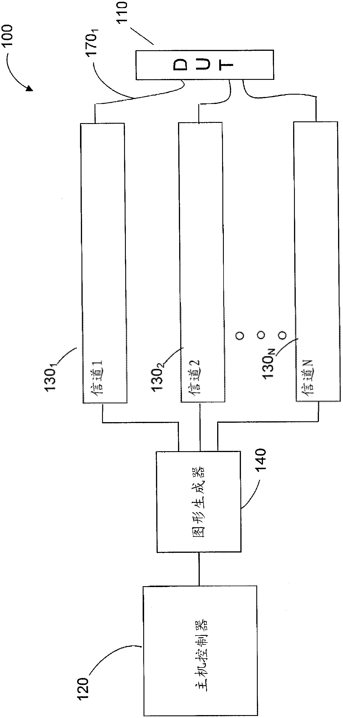
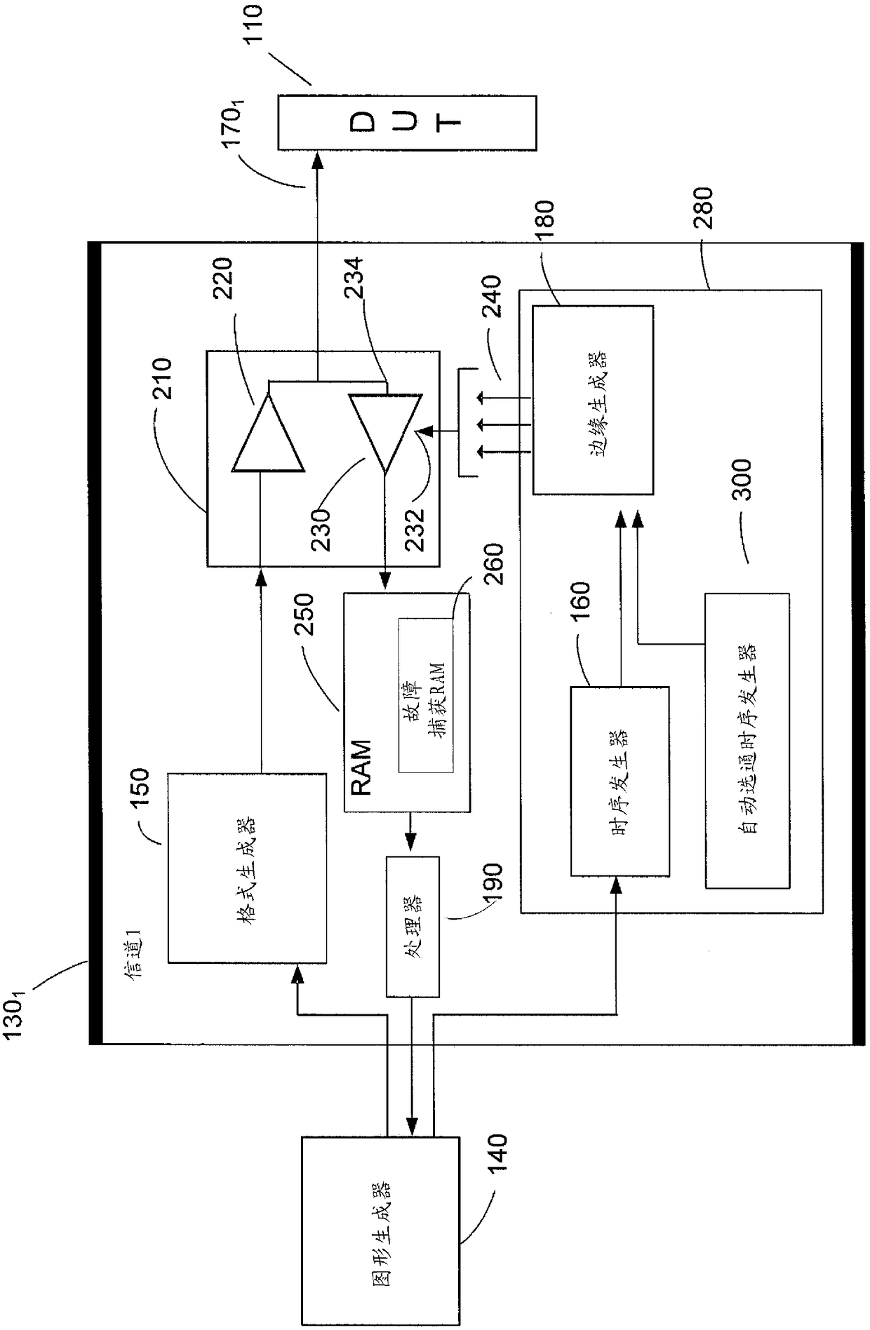
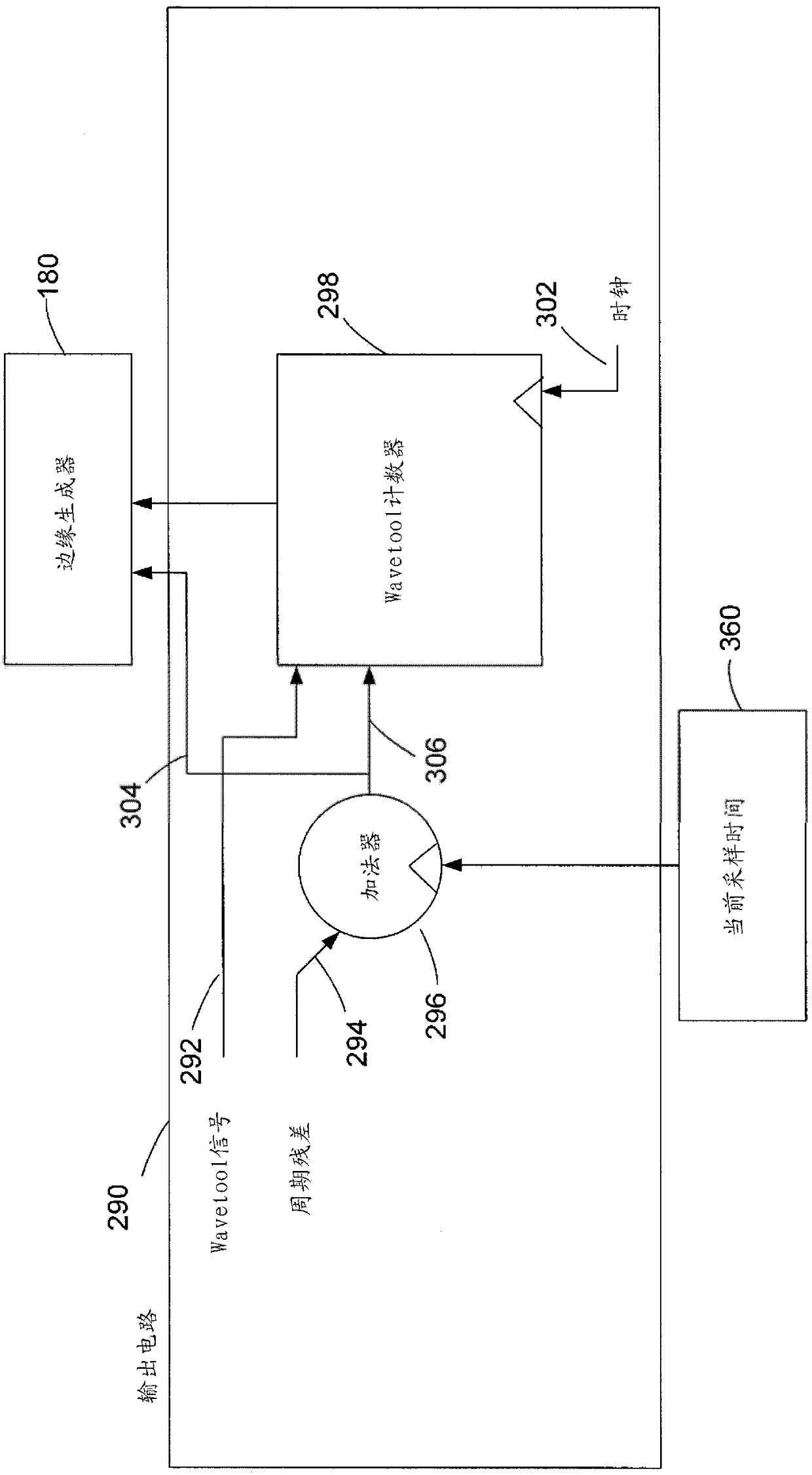
[0017] The present inventors have recognized and appreciated that an improved semiconductor device tester can reduce test development time and device test time. This improved test system enables new designs of semiconductor devices to be brought into production earlier by reducing test development time. By reducing device testing time, greater throughput in the manufacture of semiconductor devices can be achieved. Therefore, improved testers that can program faster and perform shorter tests can enhance the economics of developing semiconductor devices.

[0018] This enhanced value can be realized using a tester designed to provide a programmable method to detect the timing of signal transitions in the DUT output. Such a tester can be easily programmed by a test engineer. Alternatively or in addition, the tester can reduce the time required to run a test by accepting, as part of the programming that defines the test, a window within one repetition of the repetitive signal in ...


PUM


Abstract

A test technique that may be implemented in an automated test system for testing semiconductor devices. The test technique may enable the fast detection of a signal transition, such as an edge, within a waveform and the timing of that event. Circuitry within a digital instrument that can be quickly and flexibly programmed may, at least in part, implement the test technique. That circuitry may be simply programmed with testing parameters, such that application of the technique may lead to faster test development and faster times. In operation, that circuitry receives parameters specifying parameters of a window over a waveform in which samples of the waveform will be taken to detect the signal transition. The circuitry may convert these parameters into control signals for other components in the test system, such as an edge generator or pin electronics, to take a programmed number of samples at desired times.

Description

Background technique [0001] Automatic test equipment (ATE) (commonly referred to as "testers") is used to test semiconductor devices during their manufacture. Functional testing is typically performed by configuring the tester to apply electrical signals to multiple points on a device under test (DUT) while simultaneously measuring the output response of the DUT at certain points. [0002] In some cases, the tester is used to test the DUT to identify defects at least once during the manufacture of the DUT. The results of the test can be used to determine whether the DUT behaves as designed. If the device performs as designed, the device can be packaged and shipped to the customer. If testing indicates that the device does not perform as designed, the device is typically forwarded to further manufacturing steps, such as repair or disposal. [0003] In order to generate and measure the test signals needed to test semiconductor devices, the tester includes circuitry, sometimes...

Claims


Application Information

Patent Timeline
Patent Type & Authority Patents(China)
IPC IPC(8): H01L21/66
CPCG01R31/31922G01R31/31725G01R31/318307G01R31/318314G01R31/31926G01R31/31703G01R31/31722G01R31/31727G01R31/318594G01R31/31917G01R31/31928G01R31/31932H04L1/242H04L27/0008H04L27/2053H04L27/22H04L27/38
Inventor 罗纳德·A·萨特斯奇夫爱德华·J·森格马克·鲁本·哈特纳
Owner TERADYNE
Why Eureka
Try Eureka