Light source system, wavelength conversion device and related projection system
A technology of wavelength conversion device and light source system, which is applied to light sources, projection devices, lighting devices, etc., can solve the problems of reduced light conversion efficiency of wavelength conversion materials, low light conversion efficiency of wavelength conversion materials, etc. The effect of power density reduction
- Summary
- Abstract
- Description
- Claims
- Application Information
AI Technical Summary
Problems solved by technology
Method used
Image
Examples
Embodiment 1
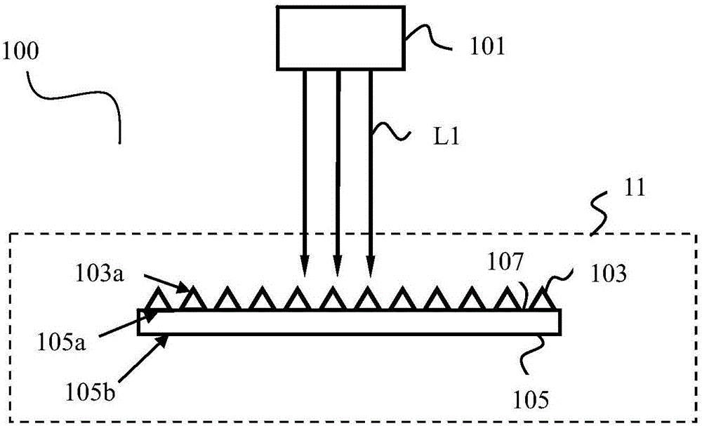
[0025] see Figure 1A , Figure 1A It is a structural schematic diagram of an embodiment of the light source system of the present invention. The light source system 100 includes an excitation light source 101 and a wavelength conversion device 11 .
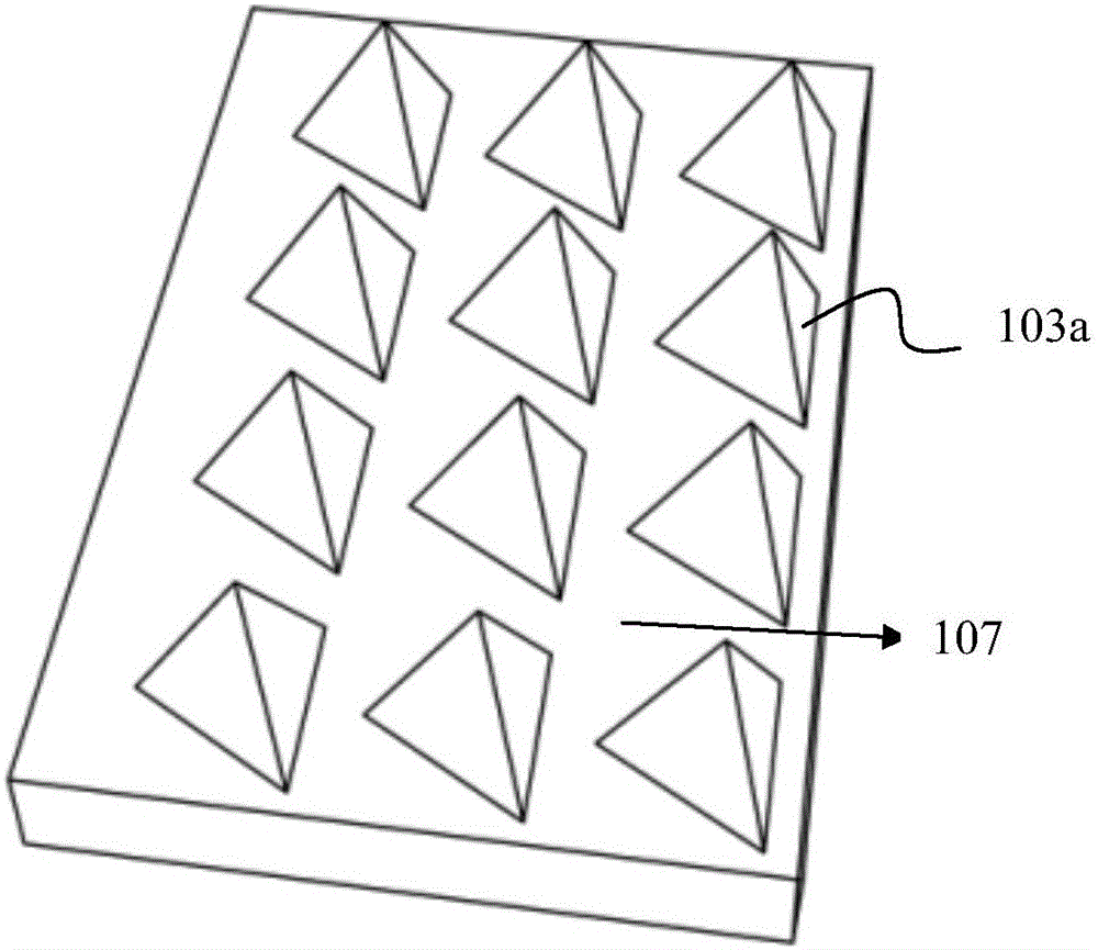
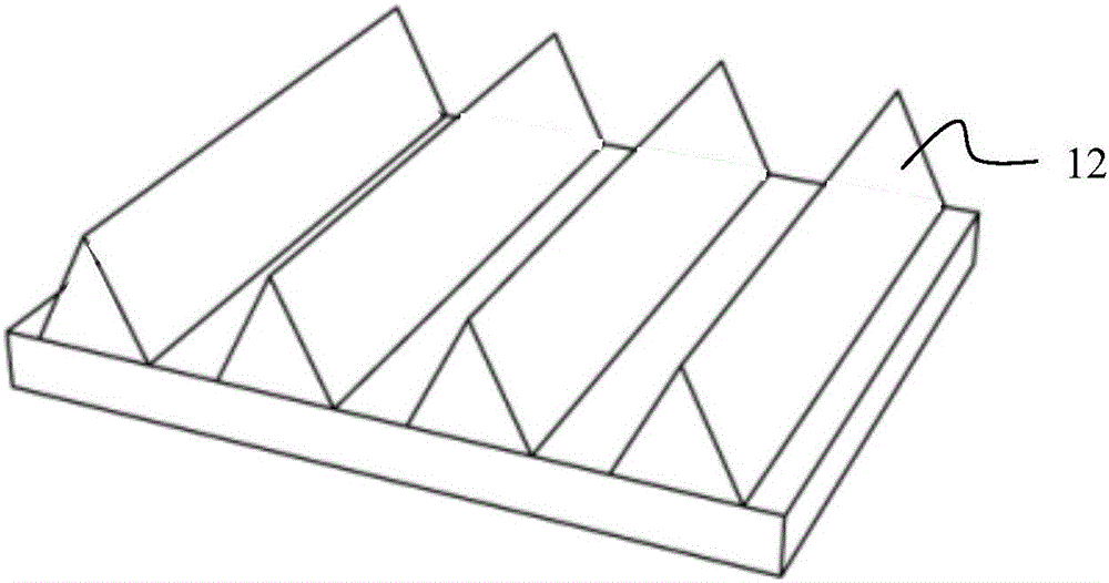
[0026] The wavelength conversion device 11 includes a microstructure array 103 . The microstructure array includes a plurality of microstructures 103a, wherein each microstructure 103a includes a wavelength conversion material for absorbing light in one wavelength range and emitting light in another wavelength range. Commonly used wavelength converting materials include phosphors. The wavelength conversion material may also be materials with wavelength conversion capabilities such as quantum dots and fluorescent dyes, and is not limited to phosphors. Such as Figure 1B as shown, Figure 1B yes Figure 1A Schematic diagram of the structure of the wavelength conversion device in the light source system shown. In this embodimen...
Embodiment 2
[0038] see image 3 , image 3 It is a structural schematic diagram of another embodiment of the light source system of the present invention. In this embodiment, the light source system 300 includes an excitation light source 301 and a wavelength conversion device 33 . The wavelength conversion device 33 includes a microstructure array 303 and a substrate 305 . Different from Embodiment 1, the base 305 in this embodiment is made of light-transmitting material, and the microstructure array 303 is disposed in the base 305 .
[0039] The substrate 305 includes a first surface 305 a and a second surface 305 b opposite to the first surface 305 a, wherein the first surface 305 a is used for receiving the excitation light L1 from the excitation light source 301 . The microstructure array 303 has an undulating side facing the first surface 305a, and the extending direction of the microstructure array 303 is parallel to the first surface 305a.
[0040] Compared with Embodiment 1, ...
Embodiment 3
[0044] see Figure 4 , Figure 4 It is a structural schematic diagram of another embodiment of the light source system of the present invention. The light source system 400 includes an excitation light source (not shown) and a wavelength conversion device 44 . The wavelength conversion device 44 includes a wavelength conversion layer 403 . Different from the above embodiments, the microstructure array in the wavelength conversion device 44 in this embodiment is not arranged on the substrate or in the substrate, but is directly formed on the side of the wavelength conversion layer 403 facing the excitation light source as in the embodiment. 1 and 2 describe microstructure arrays. Compared with the above embodiments, in this embodiment, since no substrate is needed to carry the wavelength conversion layer, the cost can be reduced.
[0045] In this embodiment, the wavelength conversion device 44 is reflective, and each microstructure is columnar. This can be achieved by coat...
PUM
 Abstract
Description
Claims
Application Information


