Light emitting diode epitaxial structure capable of shielding quantum well region polarized field effect

A technology of light-emitting diodes and epitaxial structures, applied to electrical components, circuits, semiconductor devices, etc., can solve problems such as insignificant effects, complex processes, and affecting hole transport, and achieve the effects of improving transport efficiency and internal quantum efficiency

Inactive Publication Date: 2016-08-17
HEBEI UNIV OF TECH
View PDF4 Cites 4 Cited by
  • Summary
  • Abstract
  • Description
  • Claims
  • Application Information

AI Technical Summary

Problems solved by technology

[0008] The technical problem to be solved by the present invention is to provide a light-emitting diode epitaxial structure that shields the polarization field effect in quantum wells. In order to shield the polarization field of the quantum well region, the existing technology of shielding the polarization field effect of the quantum well region has the complex process of shielding the polarization field of the quantum well region, the effect is not obvious, and it affects the space. hole transport defect

Method used


Image

  • Light emitting diode epitaxial structure capable of shielding quantum well region polarized field effect
  • Light emitting diode epitaxial structure capable of shielding quantum well region polarized field effect
  • Light emitting diode epitaxial structure capable of shielding quantum well region polarized field effect

Examples


Embodiment 1

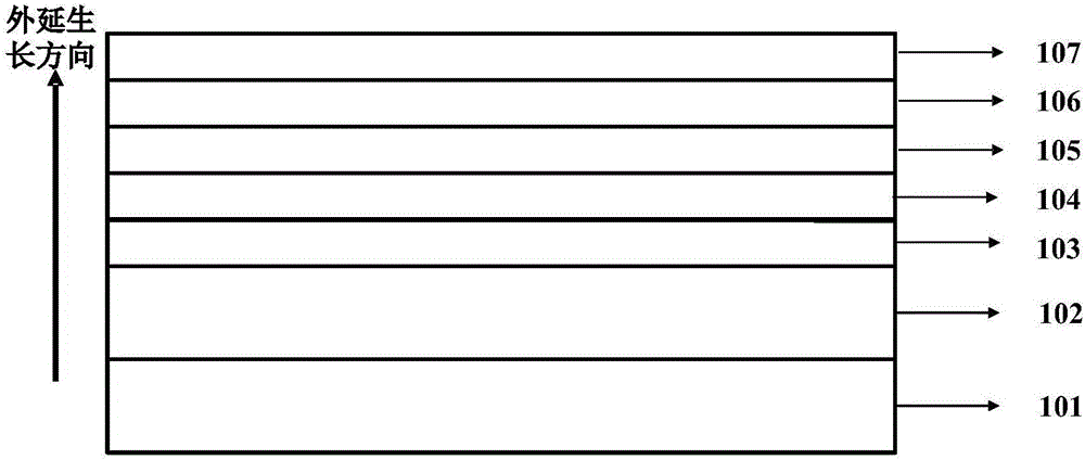
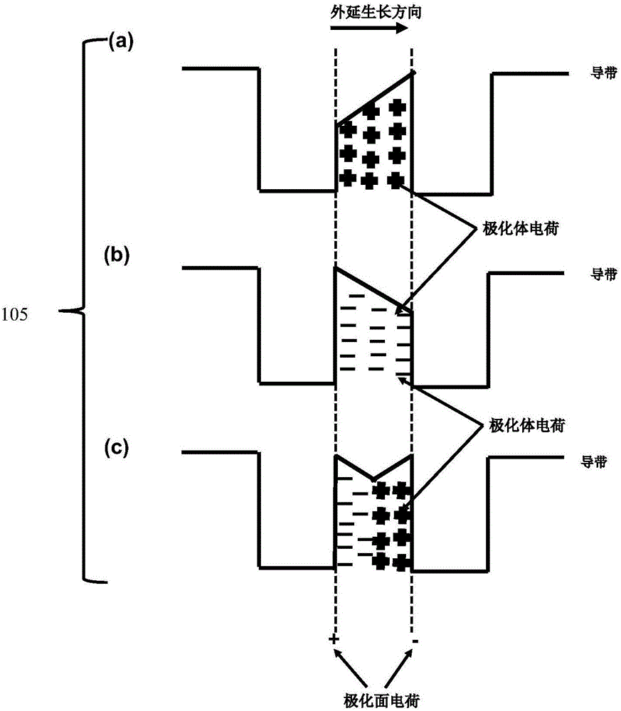
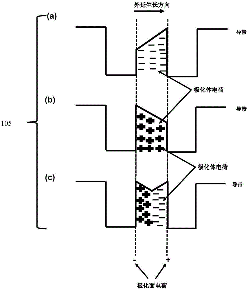
[0048] A light-emitting diode epitaxial structure shielding the polarization field effect in the quantum well of this embodiment is arranged sequentially from bottom to top: a substrate 101, a buffer layer 102, a non-doped semiconductor material layer 103, and a doped N-type semiconductor material layer 104, multi-quantum well layer 105, P-type electron blocking layer 106 and P-type semiconductor material 107; the material of the multi-quantum well layer 105 is Al 0.9 Ga 0.1 N / Al x2 Ga 1-x2 N, in the formula, x2 shows a linear change along the growth direction of [0001] in the range of 0.9≤x2≤1, and the quantum well Al 0.9 Ga 0.1 The thickness of N is 1nm, the quantum barrier Al x2 In y2 Ga 1-x2-y2 The thickness of N is 5nm, the quantum barrier Al x2 Ga 1-x2 The minimum band gap of N is larger than that of quantum well Al 0.9 Ga 0.1 The bandgap width of N.

[0049] Among the above, the substrate 101 is sapphire; the material of the buffer layer 102 is AlN, and the t...

Embodiment 2

[0060] A light-emitting diode epitaxial structure shielding the polarization field effect in the quantum well of this embodiment, the structure is arranged from bottom to top and includes: substrate 101, buffer layer 102, non-doped semiconductor material layer 103, doped N-type Semiconductor material layer 104, multi-quantum well layer 105, P-type electron blocking layer 106 and P-type semiconductor material 107; The material of described multi-quantum well layer 105 is In 0.2 Ga 0.8 N / Al x2 Ga 1-x2 N, quantum well In 0.2 Ga 0.8 The thickness of N is 5nm, the quantum barrier Al x2 Ga 1-x2 The thickness of N is 25nm, and in the formula, x2 shows a nonlinear change along the growth direction of [000-1] in the range of 0≤x2≤1, and the quantum barrier Al x2 Ga 1-x2 The minimum band gap of N is larger than the quantum well In 0.2 Ga 0.8 The bandgap width of N.

[0061] Among the above, the substrate 101 is Si; the buffer layer 102 is made of GaN with a thickness of 30nm; ...

Embodiment 3

[0072] A light-emitting diode epitaxial structure shielding the polarization field effect in the quantum well of this embodiment, the structure is arranged from bottom to top and includes: substrate 101, buffer layer 102, non-doped semiconductor material layer 103, doped N-type Semiconductor material layer 104, multi-quantum well layer 105, P-type electron blocking layer 106 and P-type semiconductor material 107; the material of described multi-quantum well layer 105 is InN / In y2 Ga 1-y2 N, in the formula, y2 shows a combination of linear change and nonlinear change along the growth direction of [0001] in the range of 0≤y2≤1. The thickness of the quantum well InN is 20nm, and the quantum barrier InN y2 Ga 1-y2 The thickness of N is 50nm, the quantum barrier In y2 Ga 1-y2 The minimum band gap of N is larger than that of the quantum well InN.

[0073] Among the above, the substrate 101 is SiC; the material of the buffer layer 102 is InN, and the thickness is 50nm; the materi...


PUM


Abstract

The invention relates to a light-emitting diode epitaxial structure shielding the polarization field effect in the quantum well, which relates to a semiconductor device specially suitable for light emission with at least one potential jump barrier or surface barrier. The structure is arranged sequentially from bottom to top, including : Substrate, buffer layer, non-doped semiconductor material layer, doped N-type semiconductor material layer, multiple quantum well layer, P-type electron blocking layer and P-type semiconductor material, wherein in the multiple quantum well layer through the quantum barrier The gradient structure is used to realize the generation of polarized body charges in the quantum barrier, which will play a role in shielding the polarization field of the quantum well region, and overcome the existing technology of shielding the polarization field effect of the quantum well region. The process of the field is complicated, the effect is not obvious, and the defect that affects the hole transport.

Description

technical field [0001] The technical solution of the invention relates to a semiconductor device specially suitable for light emission with at least one potential jump barrier or surface barrier, specifically a light emitting diode epitaxial structure shielding the polarization field effect in the quantum well. Background technique [0002] Because light-emitting diodes have the advantages of energy saving, environmental protection, and long service life, they have attracted widespread attention. At the same time, high-power white light diodes based on light-emitting diode technology have the characteristics of high brightness, high color rendering coefficient and stable color temperature, and will gradually replace incandescent and fluorescent lamps. and other traditional lighting sources. [0003] Although the light-emitting diode technology has made great progress, the current internal quantum efficiency of the light-emitting diode is still affected by the polarization fi...

Claims


Application Information

Patent Timeline
Patent Type & Authority Applications(China)
IPC IPC(8): H01L33/06H01L33/32H01L33/00H01L21/205
CPCH01L33/06H01L21/0254H01L21/0262H01L33/0075H01L33/32
Inventor 张紫辉张勇辉毕文刚徐庶耿翀
Owner HEBEI UNIV OF TECH
Why Eureka
Try Eureka