A kind of encapsulation method and encapsulation structure of high-power LED

A technology of LED packaging and packaging method, applied in the direction of semiconductor devices, electrical components, circuits, etc., can solve the problems of increasing the power of LED chips restricting the service life of high-power LEDs, reducing the luminous efficiency of LED chips, and reducing the conversion efficiency of phosphors, etc. Achieve the effect of prolonging the service life, improving the fluorescence conversion efficiency, and reducing the temperature

Inactive Publication Date: 2019-03-29
SHANGHAI GUOYU OPTOELECTRONICS TECH CO LTD
View PDF7 Cites 0 Cited by
  • Summary
  • Abstract
  • Description
  • Claims
  • Application Information

AI Technical Summary

Problems solved by technology

Since the thermal conductivity of silica gel is very low (about 1w / °C), the temperature of the LED chip is very high during actual operation, making it difficult to dissipate heat.
It will lead to two results: one is that the temperature of the LED chip is high, resulting in a decrease in the luminous efficiency of the LED chip, and the light output is reduced; the other is that the excessive temperature leads to a decrease in the conversion efficiency of the phosphor powder, resulting in a decrease in light output and a change in the color temperature of the light.
[0007] For high-power LED chips, the above defects are particularly obvious, which seriously restricts the service life of high-power LEDs and the improvement of LED chip power.

Method used


Image

  • A kind of encapsulation method and encapsulation structure of high-power LED
  • A kind of encapsulation method and encapsulation structure of high-power LED
  • A kind of encapsulation method and encapsulation structure of high-power LED

Examples


Embodiment Construction

[0039] The present invention will be further described below in conjunction with the accompanying drawings and embodiments.

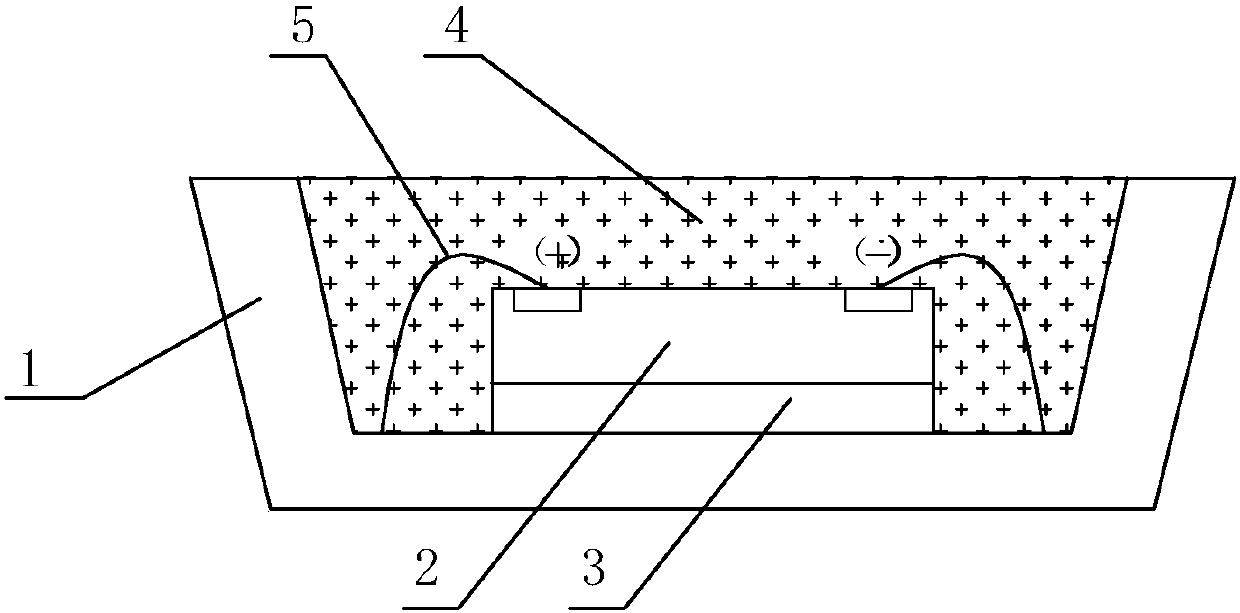
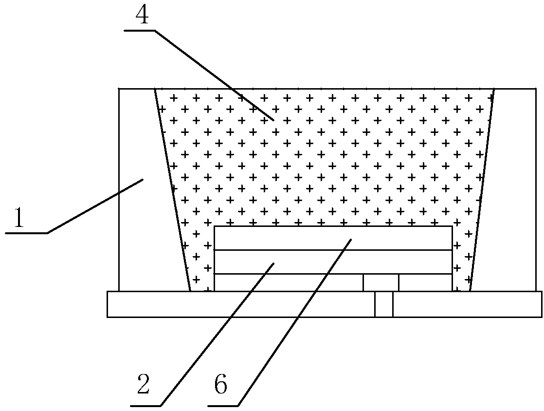
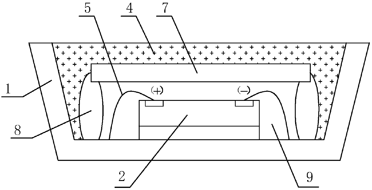
[0040] The technical solution of the present invention provides a high-power LED packaging method, the LED at least includes an LED chip arranged in a bracket or on a substrate (hereinafter referred to as a bracket) (for brevity, hereinafter referred to as image 3 LED Flip Chip in and Figure 4The formally installed LED chips are referred to as LED chips for short), and its invention points are:

[0041] Above the LED chip 2, a solid light-transmitting heat-conducting window layer 7 is arranged;

[0042] Around the LED chip, a dam 8 is set;

[0043] By setting the dam structure, the solid light-transmitting heat-conducting window layer is used as the upper base, the bracket 1 is used as the lower base, and the dam is used as the side to form a heat-conducting cavity around the LED chip. 9;

[0044] In the high-power LED packaging method, by setting...


PUM


Abstract

The invention provides a packaging method and structure of a high-power LED and belongs to field of semi-conductor devices. A solid transmitting heat conducting window layer is arranged above an LED chip. A box dam is arranged around the LED chip. By arranging a box dam structure, the solid transmitting heat conducting window layer serves as an upper bottom edge, a support or a substrate serves as a lower bottom edge, the box dam serves as a side edge, and therefore a heat conducting cavity is formed in the rim of the LED chip; by arranging the solid transmitting heat conducting window layer and constructing a heat guide cavity structure, a good heat dissipating channel is formed in the rim of the LED chip, comprehensive heat resistance is reduced, heat in the center of the LED chip can be guided out easily, the light exit rate is increased, and the service life of the low-color-temperature LED luminescent device can be prolonged greatly. The total reflection angle can be reduced, the light exit rate is increased, and the problems that an original packaging mode is low in light exit rate, and the color temperature drifts are solved. The packaging method and structure can be widely applied to the field of packaging of the LED chip and the luminescent devices.

Description

technical field [0001] The invention belongs to the field of semiconductor devices, in particular to a packaging method and packaging structure for high-power LEDs. Background technique [0002] Traditional LED packaging structures such as figure 1 As shown, the surface of the LED chip 2 is protected by a silica gel coating layer 4 to protect the LED chip and the gold wire 5, and the LED chip is fixed in the bracket 1 through the crystal-bonding glue 3. This structure is called "formal installation" in the industry. structure. [0003] The publication date is March 25, 2015. In the Chinese invention patent application with the publication number CN 104465966 A, a "white light LED packaging structure and packaging method thereof" is disclosed. The packaging structure includes a bracket 1, at least one LED flip-chip Chip 2-1, a fluorescent powder film 6, and a transparent silica gel coating layer 4, wherein the LED flip chip is arranged in the LED bracket, the positive pole ...

Claims


Application Information

Patent Timeline
Patent Type & Authority Patents(China)
IPC IPC(8): H01L33/48H01L33/58H01L33/64
CPCH01L33/48H01L33/58H01L33/644H01L2933/0033H01L2933/0058
Inventor 李抒智
Owner SHANGHAI GUOYU OPTOELECTRONICS TECH CO LTD
Why Eureka
Try Eureka