Patterned base material with emitting angle convergent and light-emitting diode element

A technology of patterned substrates and light-emitting diodes, applied in electrical components, semiconductor devices, circuits, etc., can solve problems such as affecting luminous efficiency, high defect density of gallium nitride thin films, and poor crystal quality of the active light-emitting layer, achieving increased Light extraction efficiency, the effect of good light extraction efficiency

Inactive Publication Date: 2013-11-13
GENESIS PHOTONICS
View PDF7 Cites 2 Cited by
  • Summary
  • Abstract
  • Description
  • Claims
  • Application Information

AI Technical Summary

Problems solved by technology

[0003] Generally, the traditional III-nitrides have a stable hexagonal wurtzite structure (hexagonal wurtzite structure), which is composed of two alternately mixed hexagonal close-packed (HCP) structures The hexagonal wurtzite structure includes C-plane, A-plane, M-plane and R-plane directions. Generally, the normal direction perpendicular to the C-plane is defined as (0001), and the normal direction perpendicular to the A-plane Defined as (1120), etc.; the traditional III-nitride light-emitting diode structure sequentially includes an n-type semiconductor layer, an active light-emitting layer (active layer), and a p-type semiconductor layer on the substrate, and in order to improve the components For the effect of current spreading and improving the light extraction efficiency, a transparent conductive layer (for example: indium tin oxide (ITO)) is generally arranged on the p-type semiconductor layer; finally, the p-type semiconductor layer and the n-type semiconductor layer are respectively arranged There is a p-type electrode pad and an n-type electrode pad, and the p-type electrode pad and the n-type electrode pad are respectively in ohmic contact with the p-type semiconductor layer and the n-type semiconductor layer; and in an ideal light-emitting diode, when actively emitting light After the carriers in the layer recombine into photons, if all these photons can be radiated to the outside world, then the luminous efficiency of this light-emitting diode will be 100%. However, in actual implementation, the photons generated by the active light-emitting layer may be due to various loss mechanisms. Cannot spread to the outside world with 100% luminous efficiency
[0004] For example, the above-mentioned light-emitting diodes will often cause the formation of misfit dislocations due to the strain caused by the lattice mismatch between the substrate and the epitaxial film, and some of the misfit dislocations will extend to the crystal surface, which is called Threading Dislocation; for example: there is about 16% lattice mismatch between the sapphire substrate and the gallium nitride film, resulting in a high defect density of the gallium nitride film grown on the alumina substrate, usually inside Exist 10 9 ~10 11 cm -2 The difference in density leads to poor crystal quality of the active light-emitting layer, thereby reducing the internal quantum efficiency of the light-emitting diode, thereby reducing its luminous brightness and generating heat, which increases the temperature of the light-emitting diode, thereby affecting the luminous efficiency
[0005] In addition, the light emitted by the active light-emitting layer is directed in multiple directions, so that the light-emitting angle of the light-emitting diode generally reaches between 120 degrees and 140 degrees, which not only leads to insufficient directivity of the light-emitting diode, resulting in a decrease in luminous brightness, but also Due to the large light emitting angle, when the light emitting diode is packaged in multi-chip, the light emitted by the adjacent light emitting diode elements will intersect and affect each other, and even be absorbed by the adjacent light emitting elements, resulting in a decrease in the light emitting efficiency of the light emitting diode elements

Method used


Image

  • Patterned base material with emitting angle convergent and light-emitting diode element
  • Patterned base material with emitting angle convergent and light-emitting diode element
  • Patterned base material with emitting angle convergent and light-emitting diode element

Examples


Embodiment Construction

[0038] In order to make the object, technical solution and advantages of the present invention clearer, the embodiments of the present invention will be further described in detail below in conjunction with the accompanying drawings. Here, the exemplary embodiments and descriptions of the present invention are used to explain the present invention, but not to limit the present invention.

[0039] The purpose of the present invention and its structural design and functional advantages will be described based on the preferred embodiments shown in the following drawings, so that examiners can have a deeper and more specific understanding of the present invention.

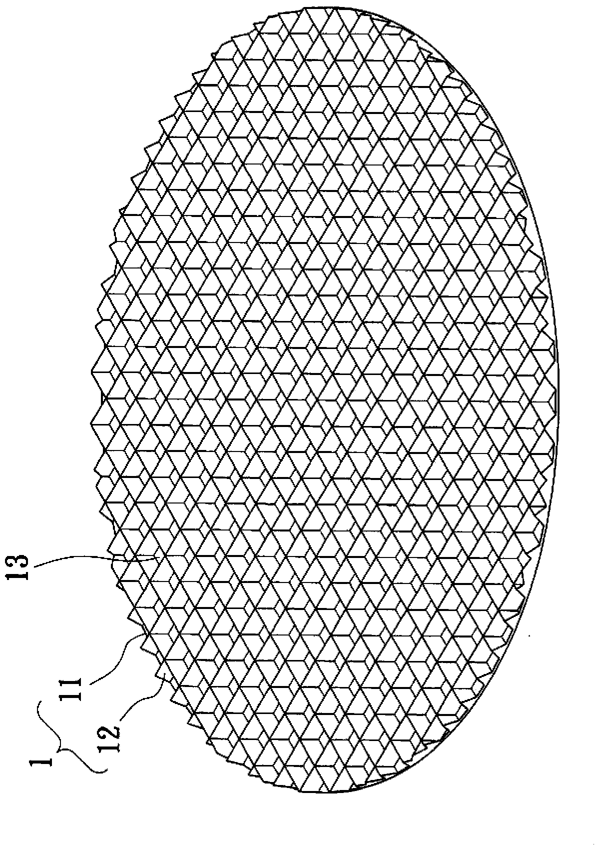
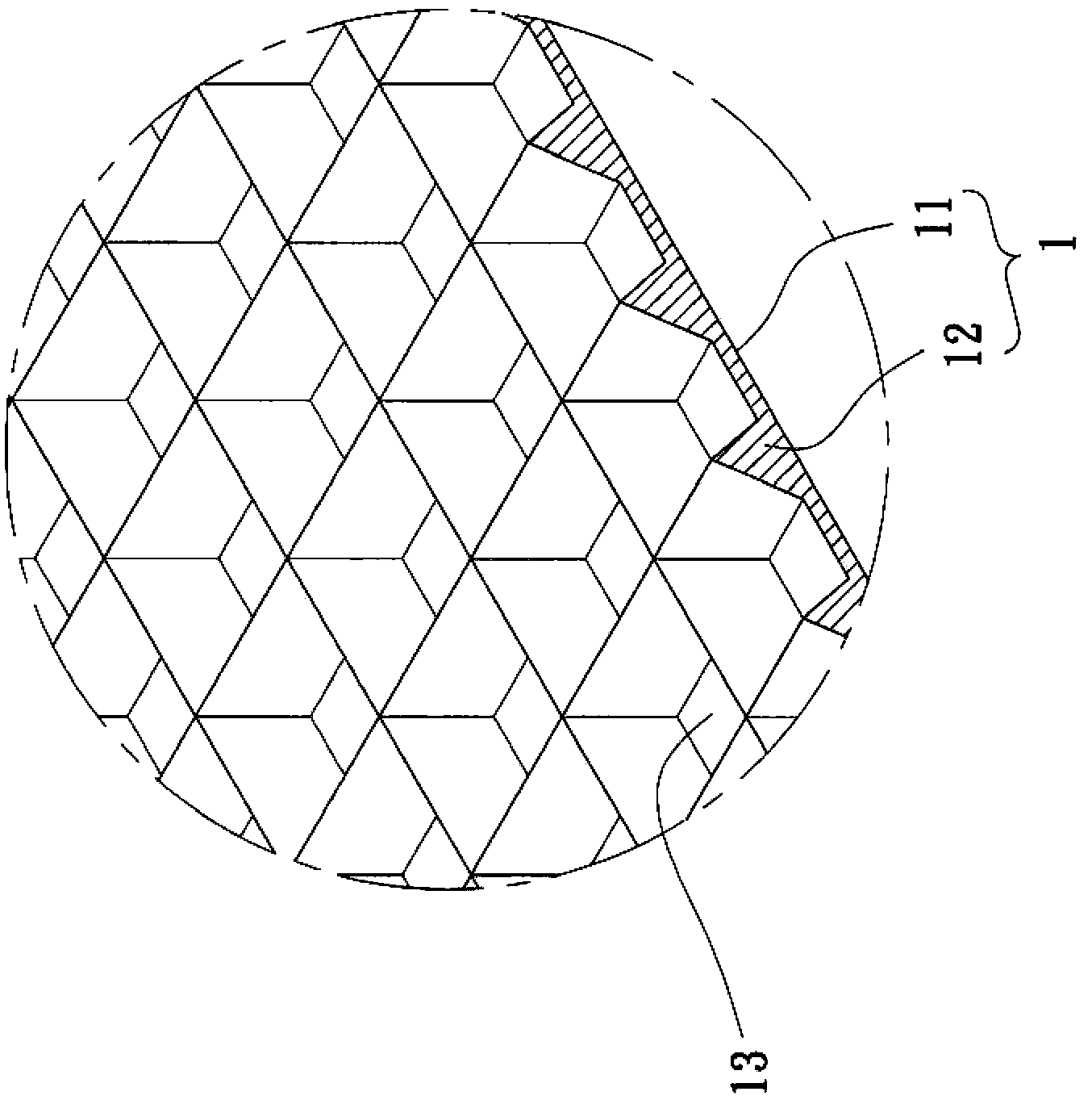
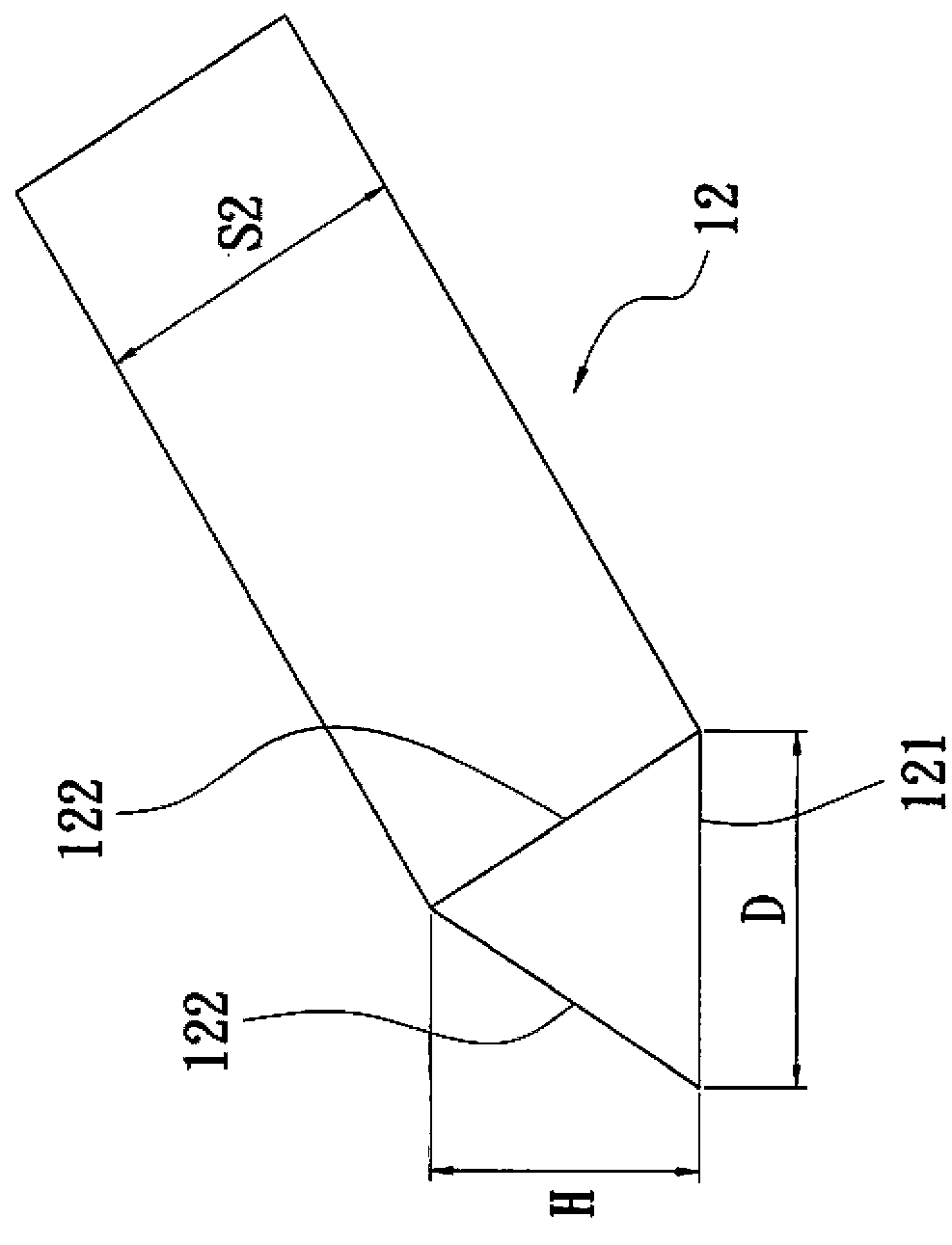
[0040] First, see Figure 1~Figure 3As shown, it is a preferred embodiment of the patterned substrate 1 with converging light emitting angles of the present invention, mainly on the surface of the substrate 11, a plurality of closed geometric shape regions 13 are provided, and the geometric shape regions 13 are compose...


PUM


Abstract

The invention discloses a patterned base material with the emitting angle convergent and a light-emitting diode element. According to the patterned base material, a plurality of closed geometric-shape regions are arranged on the surface of a substrate and are formed by being defined by at least three strip-shaped bodies, and therefore the effect of light reflection is achieved through the non-smoothness of the surface of the substrate to ensure that light is emitted from the light-emitting diode element at 100-110 degrees, perfect directivity can be achieved, and light-emitting efficiency of the light-emitting diode element made of the patterned base material can be effectively improved.

Description

technical field [0001] The invention relates to a patterned substrate and a light-emitting diode element with convergent light-emitting angles, in particular to a method of changing the direction of light and converging the light-emitting angle through a plurality of strips on the surface of the substrate, so as to increase the directivity of light and improve The light extraction efficiency of light-emitting diode components. Background technique [0002] In recent years, the application of light-emitting diodes has become more and more extensive, and has become an indispensable and important component in daily life; and light-emitting diodes are expected to replace today's lighting equipment and become the solid-state lighting components of the new generation in the future, so the development of high energy-saving, high-efficiency and Higher power light-emitting diodes will be the future trend; nitride LEDs have become one of the most emerging optoelectronic semiconductor ...

Claims


Application Information

Patent Timeline
Patent Type & Authority Applications(China)
IPC IPC(8): H01L33/20H01L33/10
Inventor 廖冠咏杨玉莲赖彦霖
Owner GENESIS PHOTONICS
Why Eureka
Try Eureka