

Light emitting diode chip with graphical structure and manufacturing method thereof
A technology of light-emitting diodes and manufacturing methods, which is applied in the field of optoelectronics, and can solve problems such as large dislocation density, decreased quantum efficiency of light-emitting diodes, and large total reflection angles, so as to reduce total reflection angles, increase light extraction efficiency, and improve crystal quality Effect
- Summary
- Abstract
- Description
- Claims
- Application Information
AI Technical Summary
Problems solved by technology
Method used
Image

Examples
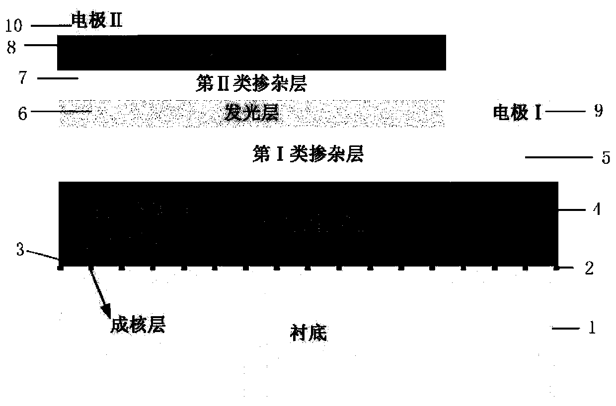
Embodiment 1
[0064] Embodiment 1 has the following characteristics and effects:
[0065] The SiO that embodiment 1 uses 2 patterned structure, characterized by SiO 2 The refractive index is 1.46, the refractive index of III-V compound is 2.5, SiO 2 A total reflection interface can be formed between the III-V compound material, and the light emitted by the light-emitting layer of the light-emitting diode propagates to the III-V compound and SiO2 When the incident angle is greater than the total reflection angle of the total reflection interface, the incident light is totally reflected and emerges from the top surface of the chip; when the incident angle is smaller than the total reflection angle, the incident light is refracted and emerges from the bottom of the LED chip substrate. The light extraction efficiency of the light emitting diode chip is increased due to total reflection of light emitted from the top and due to refraction of light emitted from the bottom. This is SiO 2 The fir...
Embodiment 2
[0067] Embodiment 2 A method for manufacturing a light-emitting diode chip with a patterned structure, its structure is as described in Embodiment 1, the difference is that the thin film material deposited on the substrate with a refractive index lower than the III-V compound is SiN x .
Embodiment 3
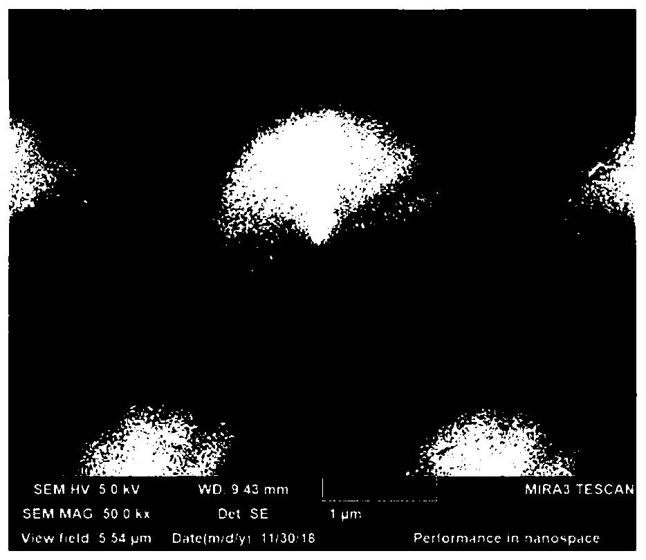
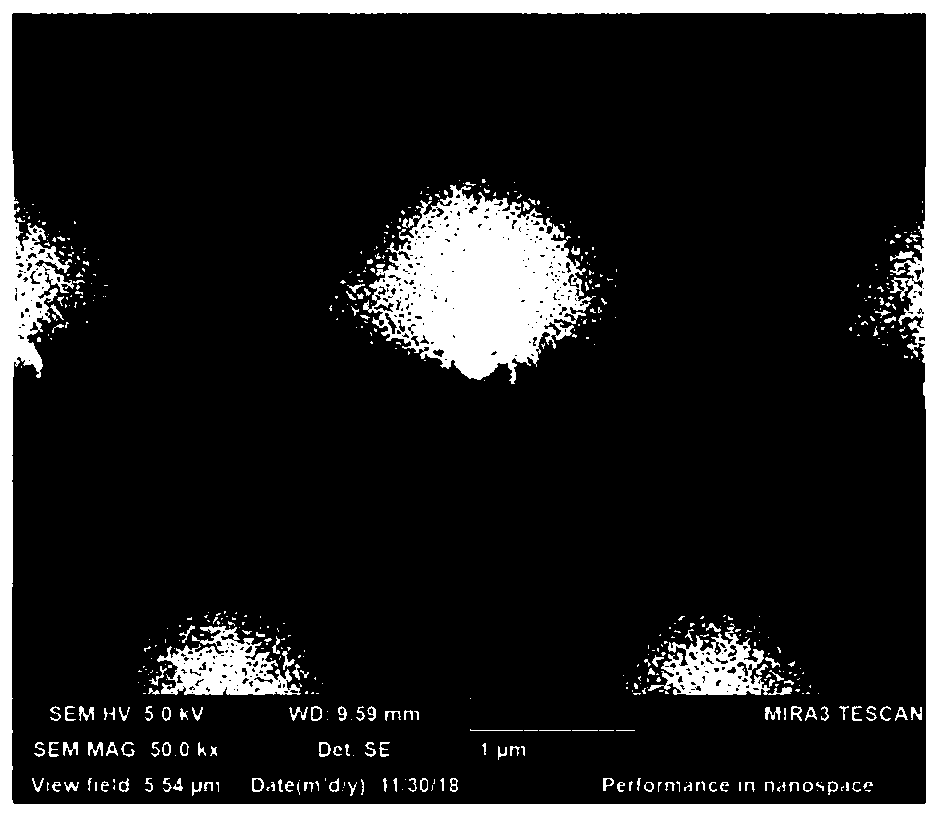
[0068] Embodiment 3 A method for manufacturing a light-emitting diode chip with a patterned structure, the method of manufacture is as described in Embodiment 1, the difference is that the patterned structure on the surface of the substrate is a quadrangular pyramid structure, and the schematic diagram of the structure is as follows Figure 7 shown.
PUM
 Abstract
Description
Claims
Application Information