Chip scale sensing chip package and a manufacturing method thereof

A technology for sensing wafers and sizes, applied in printed circuit manufacturing, semiconductor/solid-state device manufacturing, character and pattern recognition, etc., can solve problems such as defective products, damage, poor production workability of packaging substrates, etc., to avoid mismatching , the effect of reducing production costs

Active Publication Date: 2016-08-24
XINTEC INC
View PDF6 Cites 1 Cited by
  • Summary
  • Abstract
  • Description
  • Claims
  • Application Information

AI Technical Summary

Problems solved by technology

If the packaging substrate meets the requirements of miniaturization and the packaging substrate is too thin, not only the production workability of the packaging substrate is not good, but the packaging substrate is also prone to deformation due to the thickness of the packaging substrate being too thin and affected by environmental factors during the packaging process. Warped or damaged, causing problems such as defective products
[0003] In addition, touch panels or panels with sensing functions (such as biometric identification) are currently popular technology trends, but if users press the panels frequently for a long time, the touch elements located under the panels will fail

Method used


Image

  • Chip scale sensing chip package and a manufacturing method thereof
  • Chip scale sensing chip package and a manufacturing method thereof
  • Chip scale sensing chip package and a manufacturing method thereof

Examples


Embodiment 1

[0086] The following will match Figure 1A ~ Figure 1E and Figure 1C'~Figure 1E' , illustrating the wafer-scale sensing chip package module and its manufacturing method according to Embodiment 1 of the present invention.

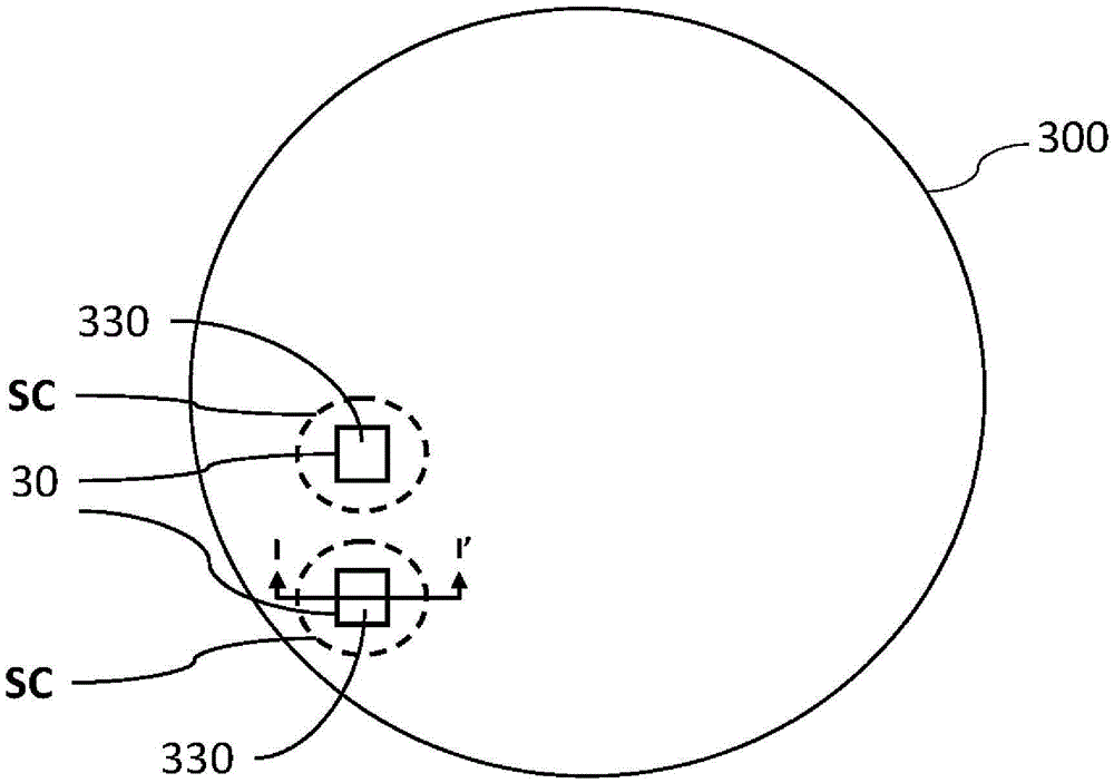
[0087] Please refer to Figure 1A Firstly, a touch panel wafer 300 is provided, the surface of which includes a plurality of die-bonding regions 30 , and a predetermined circular dicing line SC is formed on the periphery of each die-bonding region 30 . In this embodiment, the touch panel wafer 300 can be selected from a transparent material with a hardness greater than 7, such as glass.

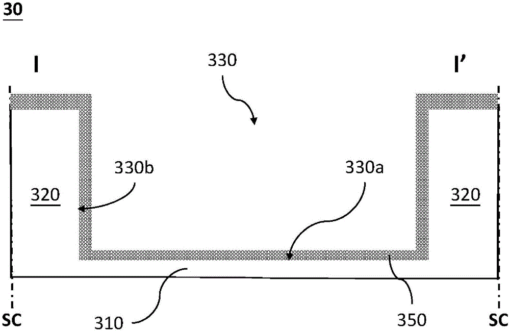
[0088] Next, please refer to Figure 1B , which is shown along the Figure 1A The cross-sectional view of the crystal-bonding region 30 presented by the cross-section line I-I'. Such as Figure 1B As shown, the crystal bonding area 30 includes a base 310 and a spacer 320 positioned on the base, the spacer 320 has a cavity 330 that exposes the surface of the base 310, ...

Embodiment 2

[0094] The following will match Figure 2A to Figure 2C and Figure 2B' to Figure 2C' , illustrating the sensing chip package module of the wafer size level and its manufacturing method according to the second embodiment of the present invention.

[0095] Please refer to Figure 2A , which shows a schematic cross-sectional view of a crystal-bonding region 50 . Such as Figure 2A As shown, the die bonding area 50 includes a base 510 and a spacer 545 on the base 510 and surrounding the base 510 , wherein the spacer 545 also includes a cavity 550 exposing the surface of the base 510 . In addition, the base 510 of this embodiment includes a touch panel 540 , a colored layer 520 and a second adhesive layer 530 sandwiched between the touch panel 540 and the colored layer 520 , and the spacer 545 is formed on the colored layer 520 .

[0096] Next, please refer to Figure 2B and Figure 2B' , through the first adhesive layer 400, so that as Figure 1C or Figure 1C' A sensor wa...


PUM


Abstract

An embodiment of this invention provides a chip scale sensing chip package module, comprising a chip scale sensing chip package, having a sensing chip with a first top substrate and a first bottom substrate opposite to the first top substrate, wherein the sensing chip has a sensing device and a plurality of conductive pads adjacent to the first top substrate, and a plurality of conductive structures connected to the conductive pads by a re-distribution layer adjacent to the first bottom surface; a touch plate having a color layer, comprising a base and a spacer formed on the base, wherein the spacer has a cavity with a bottom wall exposing part of the surface of the base and a side wall surrounding the bottom wall; and a first adhesive layer sandwich between the sensing chip and the touch plate to join the first top surface of the sensing chip to the bottom wall of the cavity of the touch plate and surround the sensing chip by the side wall of the cavity; and a print circuit board placed under the chip scale sensing chip package by bonding the conductive structure of the chip scale sensing chip package to the print circuit board.

Description

technical field [0001] The present invention relates to a sensing chip packaging module and its manufacturing method, and in particular to a sensing chip packaging module of wafer size level and its manufacturing method. Background technique [0002] The sensing device of the chip package with sensing function is easily polluted or damaged during the traditional manufacturing process, which reduces the performance of the sensing device, thereby reducing the reliability or quality of the chip package. In addition, in order to meet the trend of miniaturization of electronic products, how to reduce the thickness of the packaging substrate for carrying semiconductor chips in the packaging structure of electronic products is also an important issue in the research and development of electronic products. In the manufacturing process of the packaging substrate, it makes circuits on the thin wafer layer. If the packaging substrate meets the requirements of miniaturization and the p...

Claims


Application Information

Patent Timeline
Patent Type & Authority Applications(China)
IPC IPC(8): H01L23/13H01L23/49H01L21/60
CPCH01L23/13H01L23/49H01L24/83H01L2224/838H01L23/3121H01L23/481H01L23/525H01L2224/92242H01L2224/02371G06F3/041H01L24/02H01L24/05H01L24/13H01L24/16H01L24/29H01L24/32H01L24/92H01L24/97H05K1/0271H05K3/3436H01L2224/02377H01L2224/02381H01L2224/0401H01L2224/04105H01L2224/12105H01L2224/13024H01L2224/131H01L2224/16227H01L2224/2919H01L2224/32225H01L2224/32237H01L2224/83191H01L2224/83192H01L2224/92H01L2224/97H01L2924/15153H01L2924/15788H05K2201/0311H05K2201/10151G06F3/03547G06F2203/04103H01L24/81H01L2224/81191H01L2924/146G06V40/1306H01L2924/014H01L2224/83H01L2924/00014H01L2224/81H01L21/78
Inventor 张恕铭刘沧宇何彦仕
Owner XINTEC INC
Why Eureka
Try Eureka