Electrostatic discharge protection device

a protection device and electrostatic discharge technology, applied in the field of semiconductor devices, can solve the problems of increasing the system noise and jitter, tvs will not be able to withstand high power impact, and circuit components used in high-speed transmission interfaces can be damaged, etc., to achieve the effect of enhancing the protection capability of the same, reducing the parasitic capacitance of the bidirectional transient voltage suppressor, and low capacitance characteristics

Active Publication Date: 2020-07-21
UPI SEMICON CORP
View PDF7 Cites 0 Cited by
  • Summary
  • Abstract
  • Description
  • Claims
  • Application Information

AI Technical Summary

Benefits of technology

[0024]In view of the above, the present invention provides a bidirectional transient voltage suppressor with low capacitance characteristics. The parasitic capacitance of the bidirectional transient voltage suppressor can be reduced and the electrostatic discharge protection capability of the same can be enhanced by dividing the work area to reduce the PN junction area, adjusting the area ratio between the divided work areas and / or disposing an isolation protection structure between devices.

Problems solved by technology

Electrostatic discharge (ESD) is a significant factor causing damage to circuit components used in high-speed transmission interfaces.
Any impedance mismatch or discontinuity will increase the system's noise and jitter.
Therefore, if the junction area of the reverse biased diode is too small, the TVS will not be able to withstand high power impact.
On the other hand, if the junction area of the reverse biased diode in the TVS is increased, the parasitic capacitance is increased and the performance of the protected component itself is degraded.
This is unacceptable for the circuit components used in high-speed transmission interfaces.

Method used


Image

  • Electrostatic discharge protection device
  • Electrostatic discharge protection device
  • Electrostatic discharge protection device

Examples


Embodiment Construction

[0033]Reference will now be made in detail to the present preferred embodiments of the invention, examples of which are illustrated in the accompanying drawings. Wherever possible, the same reference numbers are used in the drawings and the description to refer to the same or like parts.

[0034]In below embodiments in which the first conductivity type is a P-type and the second conductivity type is an N-type are provided for illustration purposes, and are not construed as limiting the present invention. In another embodiment, the first conductivity type can be an N-type, and the second conductivity type can be a P-type.

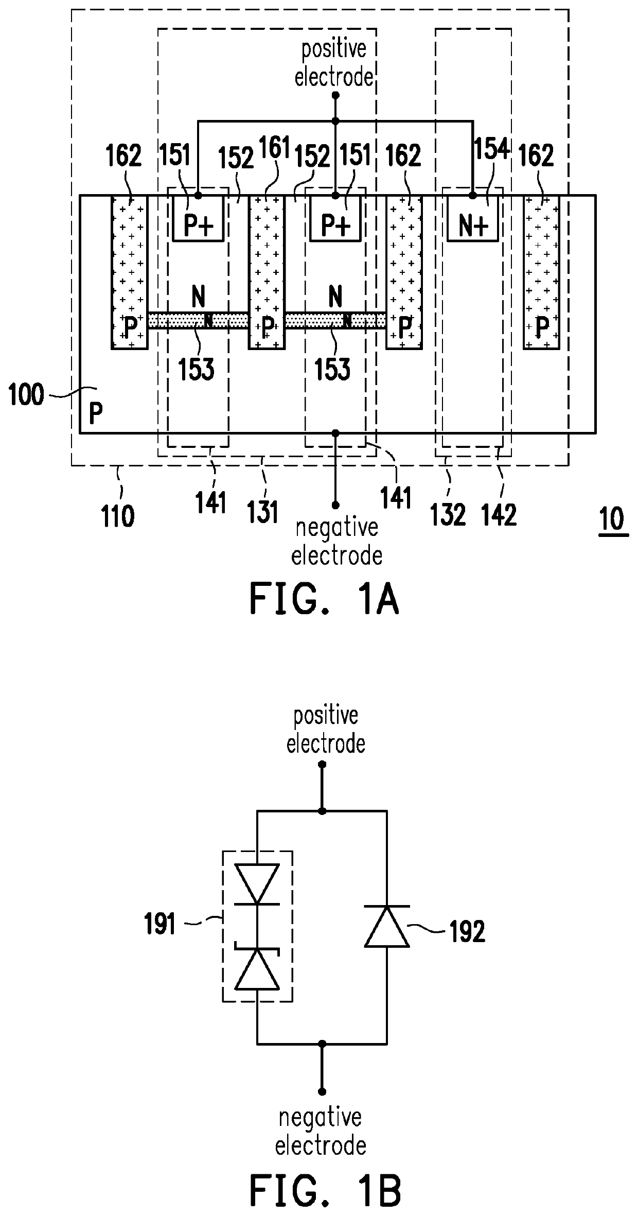
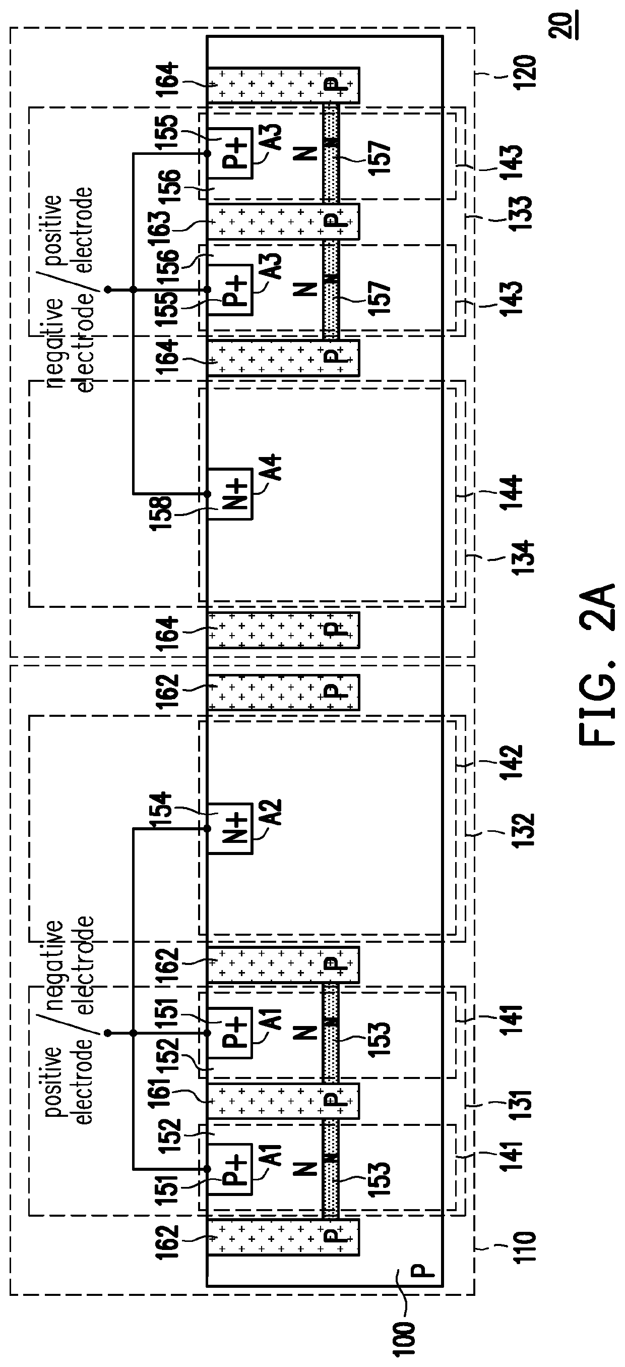
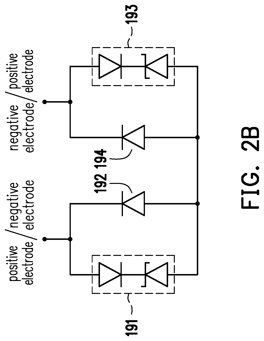
[0035]FIG. 1A illustrates a schematic cross-sectional view of an electrostatic discharge protection device according to an embodiment of the present invention. FIG. 1B illustrates an equivalent circuit diagram of an electrostatic discharge protection device according to an embodiment of the present invention.

[0036]Referring to FIG. 1A, an electrostatic discharge protect...


PUM

PropertyMeasurementUnit
widthaaaaaaaaaa
conductivity typeaaaaaaaaaa
conductivityaaaaaaaaaa

Abstract

Provided is an electrostatic discharge protection device including a first work area and a second work area. The first work area is configured to form a face-to-face connected diode string. The first work area includes a plurality of first sub-work areas. Each of the first sub-work areas includes a first doped region of a first conductivity type disposed in a substrate, a second doped region of a second conductivity type disposed in the substrate and surrounding the first doped region, and a third doped region of the second conductivity type disposed below the second doped region. The second work area is configured to form at least one diode. The second work area includes at least one second sub-work area. The second sub-work area includes a fourth doped region of the second conductivity type disposed in the substrate. Besides, the fourth doped region is electrically connected to the first doped region.

Description

CROSS-REFERENCE TO RELATED APPLICATION[0001]This application claims the priority benefit of Taiwan application serial no. 107119394, filed on Jun. 5, 2018. The entirety of the above-mentioned patent application is hereby incorporated by reference herein and made a part of this specification.BACKGROUND OF THE INVENTIONField of Invention[0002]The present invention relates to a semiconductor device, and more generally to an electrostatic discharge protection device having an electrostatic discharge protection function.Description of Related Art[0003]Electrostatic discharge (ESD) is a significant factor causing damage to circuit components used in high-speed transmission interfaces. In order to avoid damage from electrostatic discharge, an electrostatic discharge protection device must be placed between the input and output terminals. However, as the applications of electronic devices are developed, data is required to transmit faster and faster at the transmission interfaces. Any imped...

Claims


Application Information

Patent Timeline
Patent Type & Authority Patents(United States)
IPC IPC(8): H01L27/02H01L29/861H01L27/08H05K1/02H01L29/06
CPCH01L29/861H01L29/0649H01L27/0255H05K1/0259H01L27/0814H01L29/0646
Inventor CHENHSU, MING-CHUNCHEN, CHIH-HAO
Owner UPI SEMICON CORP
Why Eureka
Try Eureka