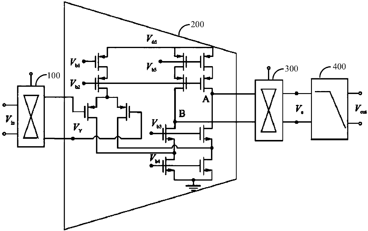
A Weak Signal Readout Circuit
A technology for reading out circuits and weak signals, applied in logic circuit interface devices, logic circuit connection/interface layout, etc., can solve the large offset voltage of operational amplifiers, affect weak signal detection and readout, and cannot be filtered by low-frequency filter 400 And other issues
- Summary
- Abstract
- Description
- Claims
- Application Information
AI Technical Summary
Problems solved by technology
Method used
Image
Examples
Embodiment 1
[0090] see image 3 , which is a schematic diagram of Embodiment 1 of the weak signal readout circuit provided by the present invention.
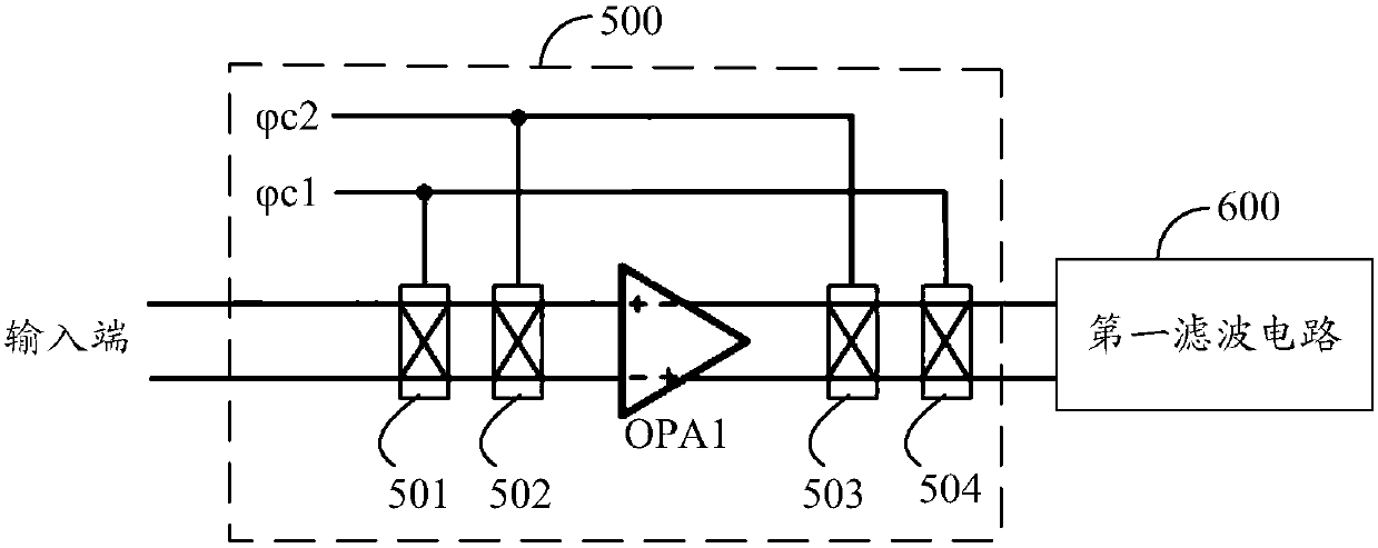
[0091] The weak signal readout circuit provided in this embodiment includes: a chopper amplifier circuit 500;
[0092] The chopper amplifier circuit 500 includes: a first chopper 501, a second chopper 502, a third chopper 503, a fourth chopper 504 and a first operational amplifier OPA1;
[0093] The input terminal of the first chopper 501 is connected to a weak signal, the positive pole of the output terminal of the first chopper 501 is connected to the positive pole of the input terminal of the second chopper 502, and the positive pole of the input terminal of the first chopper 501 The negative pole of the output terminal is connected to the negative pole of the input terminal of the second chopper 502;
[0094] The positive pole of the output terminal of the second chopper 502 is connected to the positive input terminal of the first ope...
Embodiment 2
[0111] see Figure 4 , which is a schematic diagram of Embodiment 2 of the weak signal readout circuit provided by the present invention. Compared to image 3 , this embodiment provides a more specific schematic diagram of a weak signal readout circuit.
[0112] The chopping amplifier circuit 500 further includes: a second operational amplifier OPA2, a third operational amplifier OPA3, a first resistor R1, a second resistor R2, a first capacitor C1, a second capacitor C2, and a third capacitor C3;
[0113] The chopping amplifier circuit 500 adopts a negative feedback structure to ensure the gain accuracy of the chopping amplifier circuit.
[0114] The positive phase input terminal of the second operational amplifier OPA2 is connected to the negative pole of the output terminal of the fourth chopper 504, and the inverting input terminal of the second operational amplifier OPA2 is connected to the negative pole of the output terminal of the fourth chopper 504. positive pole, ...
Embodiment 3
[0171] see Figure 6 , which is a schematic diagram of Embodiment 3 of the weak signal readout circuit provided by the present invention.
[0172] The weak signal readout circuit provided in this embodiment further includes: a first filter circuit 600;
[0173] The first filter circuit 600 is used to filter out harmonic components whose frequency is greater than a first preset frequency in the output signal of the chopper amplifier circuit 500;
[0174] The first preset frequency is greater than the frequency of the weak signal.
[0175] The first filter circuit 600 can filter out noise and offset voltage in the output signal of the chopper amplifier circuit 500 .
[0176] It can be understood that there are many filter circuit topologies with various structures, all of which can perform the above-mentioned filtering function. The topological structure of one of the filter circuits will be introduced below, and the other circuit topological structures will not be repeated h...
PUM
 Abstract
Description
Claims
Application Information


