DQPSK (Differential Quadrature Phase Shift Keying) demodulation device
A demodulation device and differential four-phase technology, applied in the field of optical signal demodulation, can solve the problems of affecting the accuracy of the demodulation device, increasing the size of the demodulation device, affecting the refractive index, etc., and achieving easy control, energy saving, and accurate control. Effect
- Summary
- Abstract
- Description
- Claims
- Application Information
AI Technical Summary
Problems solved by technology
Method used
Image

Examples
Embodiment 1
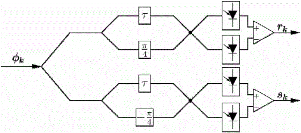
[0045] The invention provides a device and a method for demodulating DQPSK signals with a 40Gbaud baud rate by utilizing the optical force in the optical waveguide.
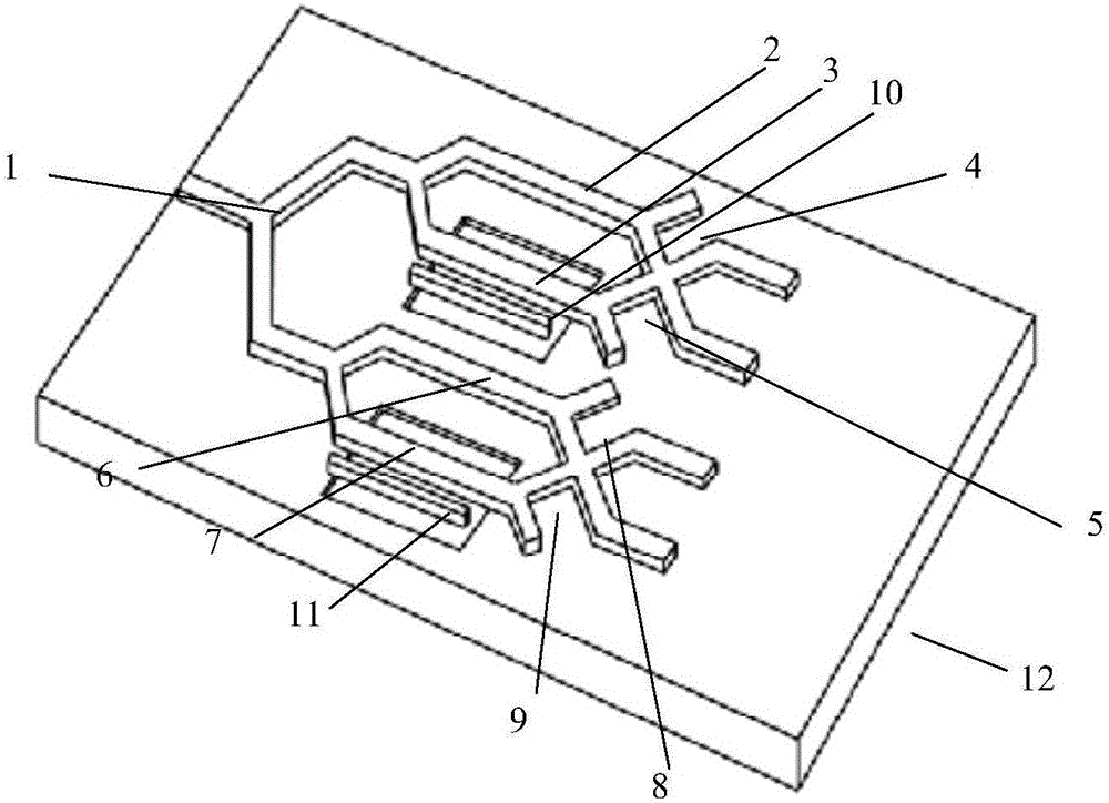
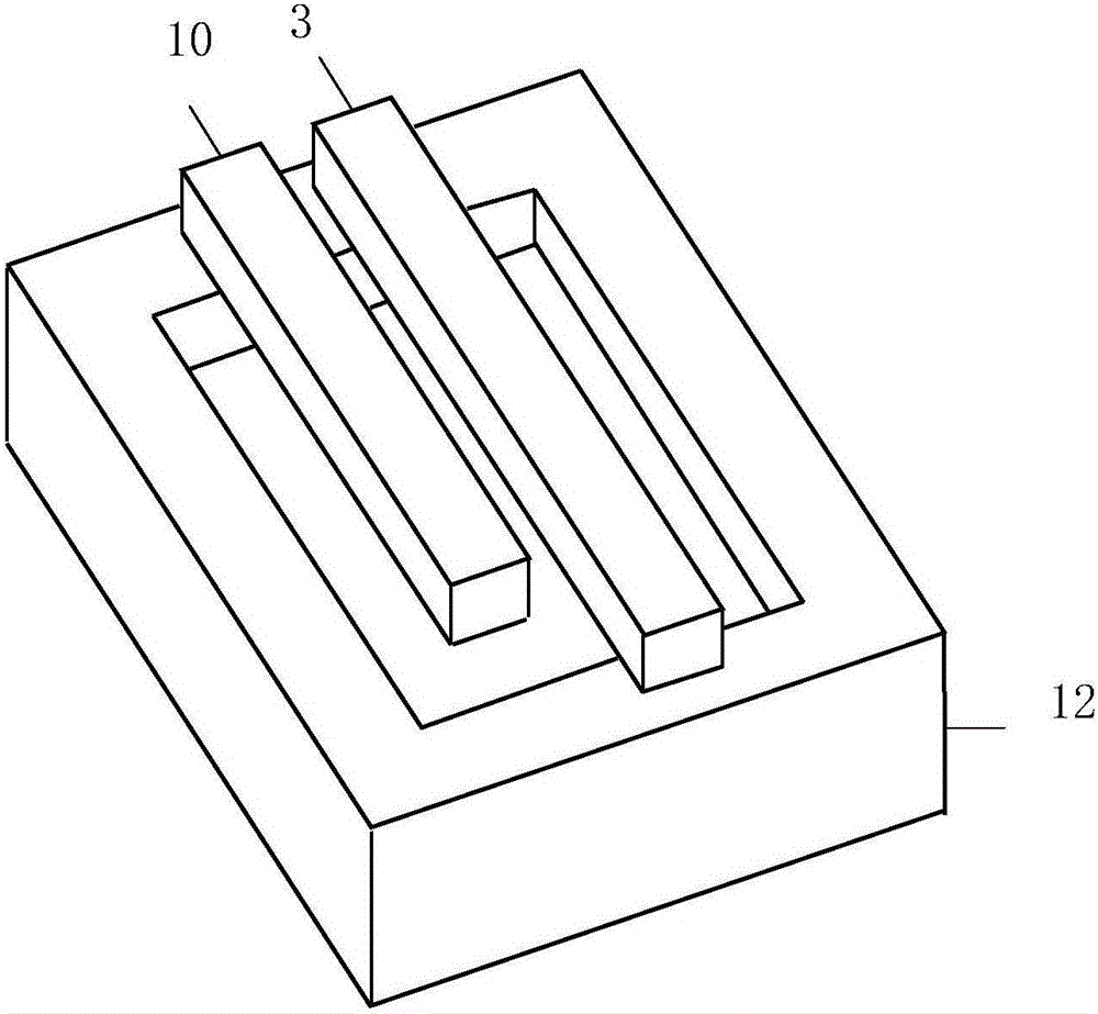
[0046] Such as figure 2 As shown, the structure of the demodulation device that utilizes the optical force in the optical waveguide to demodulate the 40Gbaud baud rate DQPSK signal provided by the present invention includes a first Mach-Zehnder interferometer attached to the substrate 12, Second Mach-Zehnder interferometer, 3dB coupler 1, first 99:1 coupler 4, second 99:1 coupler 5, third 99:1 coupler 8, fourth 99:1 coupler 9, The first nanowire 10 is hollowed out on the contact surface with the substrate, and the second nanowire 11 is hollowed out on the contact surface with the substrate. The upper arm of the first Mach-Zehnder interferometer is the first waveguide 2 attached to the substrate, the lower arm is the second waveguide 3 attached to the substrate; the upper arm of the second Mach-Zehnder interfero...
Embodiment 2
[0061]Fig. 7 has provided the expansion of the present invention, and the demodulation device structure that is used to carry out 40 / 20 / 10Gbaud baud rate DQPSK signal demodulation comprises the first Mach-Zehnder interferometer that is attached on the substrate 12, the second Mach -Zehnder interferometer, 3dB coupler 1, first 99:1 coupler 4, second 99:1 coupler 5, third 99:1 coupler 8, fourth 99:1 coupler 9, and substrate The first nanowire 10 is hollowed out at the contact surface, and the second nanowire 11 is hollowed out at the contact surface with the substrate. The lower arm of the first Mach-Zehnder interferometer is the second waveguide 3 attached to the substrate; the upper arm of the second Mach-Zehnder interferometer is the third waveguide 6 attached to the substrate, and the lower arm is attached to the substrate. The fourth waveguide 7 on the bottom. The first 99:1 coupler 4 is connected to the first waveguide 2 of the upper arm of the first Mach-Zehnder interfer...
PUM
| Property | Measurement | Unit |
|---|---|---|
| Depth | aaaaa | aaaaa |
| Height | aaaaa | aaaaa |
| Width | aaaaa | aaaaa |
Abstract
Description
Claims
Application Information
 - R&D
- Intellectual Property
- Life Sciences
- Materials
- Tech Scout
- Unparalleled Data Quality
- Higher Quality Content
- 60% Fewer Hallucinations
Browse by: Latest US Patents, China's latest patents, Technical Efficacy Thesaurus, Application Domain, Technology Topic, Popular Technical Reports.
© 2025 PatSnap. All rights reserved.Legal|Privacy policy|Modern Slavery Act Transparency Statement|Sitemap|About US| Contact US: help@patsnap.com