3d global pixel unit and preparation method thereof

A pixel unit, global technology, used in electrical components, radiation control devices, semiconductor/solid-state device manufacturing, etc., can solve the problem of photosensitive units, storage capacitors and readout circuits easily interfering with each other, to improve optical isolation, improve Light path, the effect of reducing the chip area

Active Publication Date: 2019-06-21
SHANGHAI INTEGRATED CIRCUIT RES & DEV CENT +1
View PDF3 Cites 2 Cited by
  • Summary
  • Abstract
  • Description
  • Claims
  • Application Information

AI Technical Summary

Problems solved by technology

Moreover, the photosensitive unit, the storage capacitor and the readout circuit tend to interfere with each other

Method used


Image

  • 3d global pixel unit and preparation method thereof
  • 3d global pixel unit and preparation method thereof
  • 3d global pixel unit and preparation method thereof

Examples


Embodiment Construction

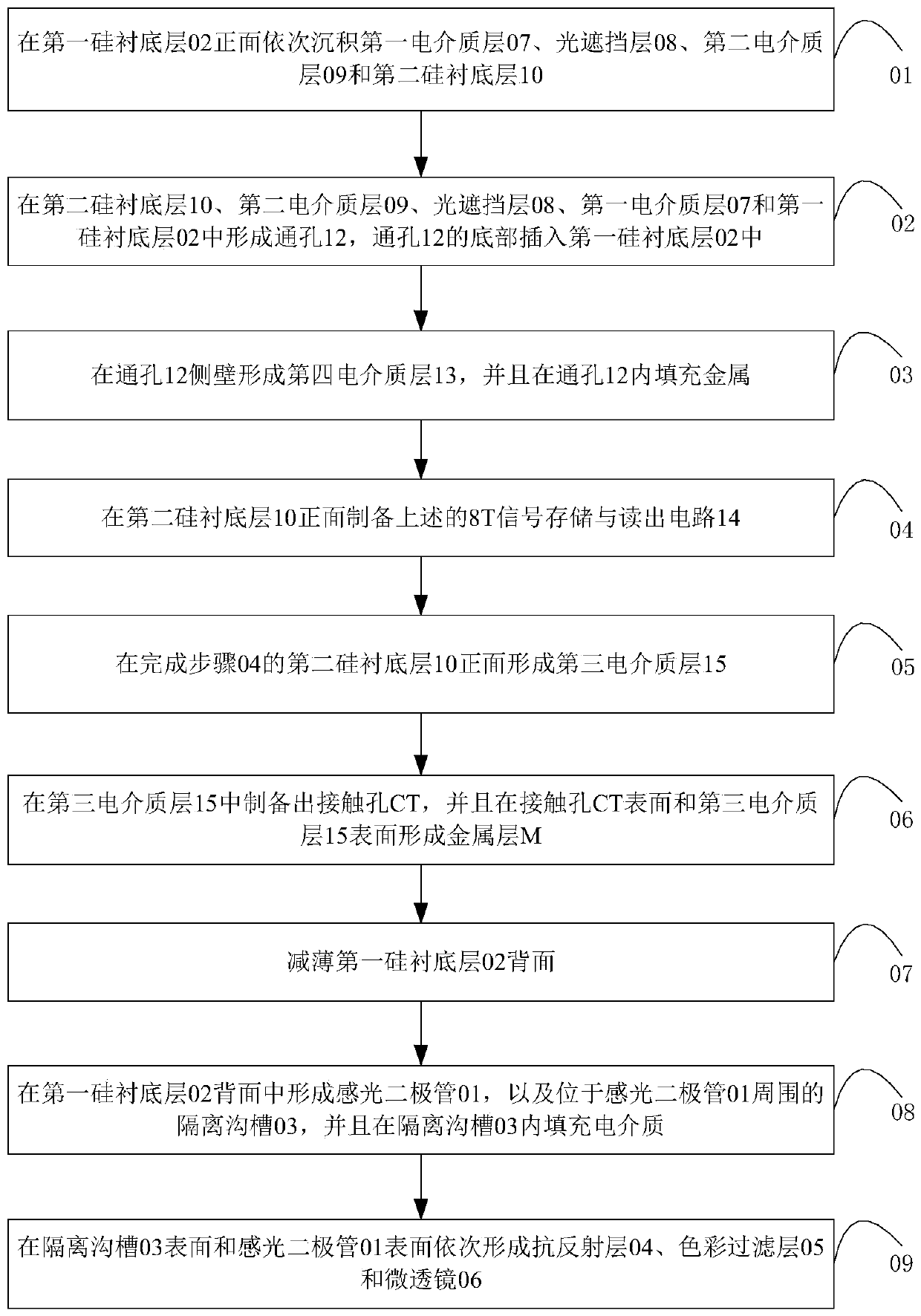
[0039] In order to make the content of the present invention clearer and easier to understand, the content of the present invention will be further described below in conjunction with the accompanying drawings. Of course, the present invention is not limited to this specific embodiment, and general replacements known to those skilled in the art are also covered within the protection scope of the present invention.

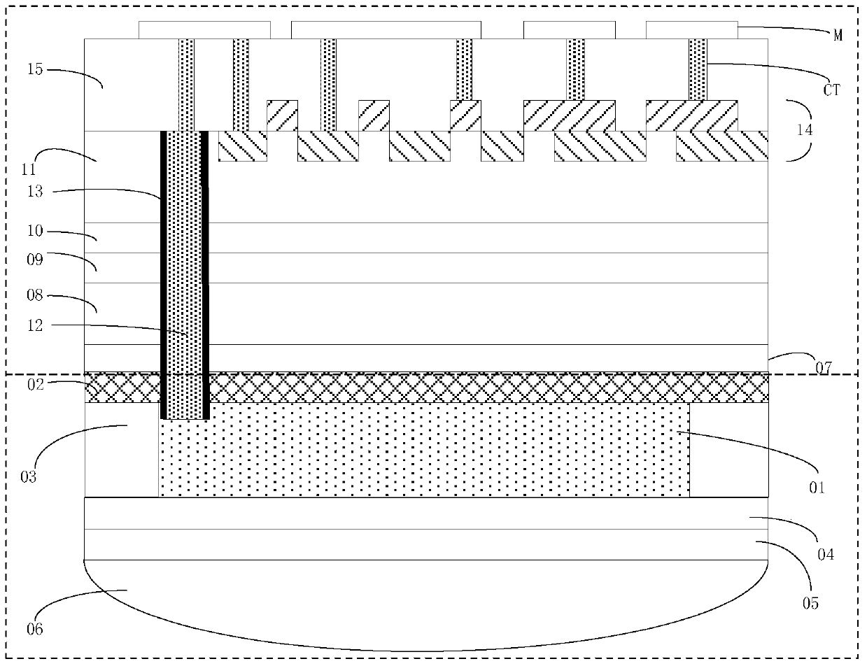
[0040]In the present invention, the photosensitive area of ​​the first silicon substrate layer and the signal storage and readout circuit unit area of ​​the second silicon substrate layer are arranged in the vertical direction, and the photosensitive diode is located above the signal storage and readout circuit; Realize the interconnection between the photosensitive diode and the signal storage and readout circuit.

[0041] The following is attached Figure 1-12 The present invention will be described in further detail with specific examples. It should be noted t...


PUM


Abstract

The invention provides a 3D global pixel unit and a preparation method therefor. The 3D global pixel unit comprises a light-sensitive region manufactured on a first silicon substrate layer, and a 8T signal storage and reading circuit region manufactured on a second silicon substrate layer; the light-sensitive region and the 8T signal storage and reading circuit region are arranged in a vertical direction; the interconnection of the light-sensitive region and the 8T signal storage and reading circuit region is realized through connection of through holes; a reset switch and a transmission pipe are stored on a first storage node and a second storage node through a first switch tube and a second switch tube based on a certain time sequence; and finally, the signal voltage obtained in the exposure time is stored in the pixel unit for a certain time and then is read out, so that the global shutter exposure of the overall pixel unit array is realized consequently. According to the 3D global pixel unit, the perpendicular interconnection of the reading circuit and the light-sensitive diode is realized; and therefore, the light access between the external and the light-sensitive diode is improved, the optical isolation degree of a signal storage capacitor is improved, and the occupied chip area of the pixel unit is reduced as well.

Description

technical field [0001] The invention relates to the technical field of semiconductor image sensing, in particular to a 3D global pixel unit and a preparation method thereof. Background technique [0002] Traditional global shutter pixel technology is mainly used in CCD image sensors. Due to the increasing popularity of CMOS image sensors, and because machine vision, film production, industrial, automotive, and scanning applications must capture fast-moving objects with high Traditional barriers associated with shutter pixel technology. With this effort, the provided global shutter pixel technology has smaller pixel size, larger fill factor, lower dark current, and lower noise, making CMOS image sensors the preferred choice for CCD sensors in more applications. Viable alternatives. [0003] In the global shutter pixel unit of a conventional CMOS image sensor, the photosensitive diode and the signal storage and readout circuit unit devices are all made in the same plane. T...

Claims


Application Information

Patent Timeline
Patent Type & Authority Patents(China)
IPC IPC(8): H01L27/146H01L21/768
CPCH01L21/768H01L27/146H01L27/14605H01L27/14636
Inventor 赵宇航
Owner SHANGHAI INTEGRATED CIRCUIT RES & DEV CENT
Why Eureka
Try Eureka