High voltage JFET device and processing method of the same
A process method and device technology, applied in the field of high-voltage JFET devices, can solve problems such as concentration reduction, achieve the effects of reducing pinch-off voltage, increasing breakdown voltage, and simple implementation
- Summary
- Abstract
- Description
- Claims
- Application Information
AI Technical Summary
Problems solved by technology
Method used
Image
Examples
Embodiment Construction
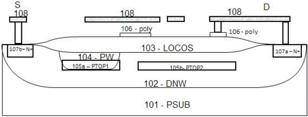
[0026] High voltage JFET device described in the present invention, such as Figure 8 As shown, there is an N-type deep well 102 in the P-type substrate 101. From the cross-sectional perspective, the field oxygen 103 is above the N-type deep well 102, and the two ends of the field oxygen 103 are the source region 107b and the drain region of the JFET respectively. 107 a , the field oxygen 103 covers the polysilicon field plate 106 .
[0027] The N-type deep well 102 is divided into two sections, the first N-type deep well and the second N-type deep well, such as Figure 8 As shown in , the first N-type deep well 102 on the left side includes the source region 107b of the JFET, and the second N-type deep well 102 on the right side includes the drain region 107a of the JFET and the P-type injection layer 105b; the first The N-type deep well and the second N-type deep well are independent of each other, with a certain distance between them, generally 2-6 μm, and the distance can...
PUM
 Abstract
Description
Claims
Application Information
 - R&D
- Intellectual Property
- Life Sciences
- Materials
- Tech Scout
- Unparalleled Data Quality
- Higher Quality Content
- 60% Fewer Hallucinations
Browse by: Latest US Patents, China's latest patents, Technical Efficacy Thesaurus, Application Domain, Technology Topic, Popular Technical Reports.
© 2025 PatSnap. All rights reserved.Legal|Privacy policy|Modern Slavery Act Transparency Statement|Sitemap|About US| Contact US: help@patsnap.com


