Semiconductor structure and forming method thereof

A semiconductor and substrate technology, which is applied to the semiconductor structure with high dielectric constant gate dielectric and the field of its formation, to achieve the effect of reducing gate leakage current

Active Publication Date: 2016-09-07
INST OF MICROELECTRONICS CHINESE ACAD OF SCI
View PDF4 Cites 5 Cited by
  • Summary
  • Abstract
  • Description
  • Claims
  • Application Information

AI Technical Summary

Problems solved by technology

And the traditional rapid thermal anneal (rapidthermal anneal) process time is 15-60 seconds

Method used


Image

  • Semiconductor structure and forming method thereof
  • Semiconductor structure and forming method thereof

Examples


Embodiment Construction

[0015] In order to make the object, technical solution and advantages of the present invention clearer, the embodiments of the present invention will be described in detail below with reference to the accompanying drawings.

[0016] Embodiments of the present invention are described in detail below, examples of which are shown in the drawings, wherein the same or similar reference numerals designate the same or similar elements or elements having the same or similar functions throughout. The embodiments described below by referring to the figures are exemplary only for explaining the present invention and should not be construed as limiting the present invention.

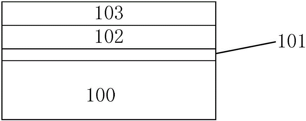
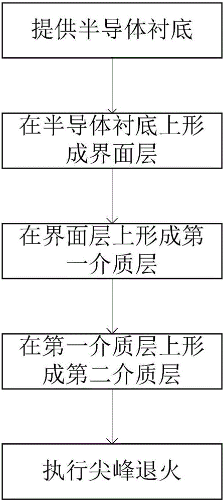
[0017] Below in conjunction with accompanying drawing and embodiment, refer to figure 1 The present invention is described in further detail, wherein, figure 1 is a schematic diagram of a semiconductor structure according to one embodiment of the present invention. figure 1 The shown semiconductor structure includ...


PUM


Abstract

The invention provides a semiconductor structure, which comprises a semiconductor substrate, an interface layer, a first dielectric layer and a second dielectric layer, wherein the interface layer is formed on the semiconductor substrate; the first dielectric layer is formed on the interface layer; the second dielectric layer is formed on the first dielectric layer; and the phase-transition temperature of the second dielectric layer is lower than that of the first dielectric layer. By the semiconductor structure and the forming method thereof provided by the invention, the condition that external oxygen diffuses and passes through the second dielectric layer and enters the first dielectric layer is facilitated when dielectric constants of the dielectric layers are improved; and oxygen vacancies in the first dielectric layer are reduced, so that a gate leakage current is reduced.

Description

technical field [0001] The invention relates to the field of integrated circuit manufacturing, more specifically, to a semiconductor structure with a high dielectric constant gate dielectric and a forming method thereof. Background technique [0002] As the feature size of metal-oxide-semiconductor field-effect transistors (MOSFETs) continues to shrink according to Moore's Law, the gate dielectric layer (usually SiO 2 or SiON) is also scaled down to the nanometer level. When the thickness of the gate dielectric layer is thinned to a certain extent, due to the influence of quantum tunneling effect and the diffusion of impurities in the gate electrode to the substrate, the gate leakage current will increase significantly, which will increase the power consumption of the device and seriously affect the performance of the device. stability and reliability. High-k materials have been used instead of SiO in the prior art 2 Form the gate dielectric. Using a high-k material as t...

Claims


Application Information

Patent Timeline
Patent Type & Authority Applications(China)
IPC IPC(8): H01L29/51H01L21/28
CPCH01L21/28158H01L21/28185H01L29/513
Inventor 马雪丽王文武赵超
Owner INST OF MICROELECTRONICS CHINESE ACAD OF SCI
Why Eureka
Try Eureka