
Semiconductor device

A semiconductor and housing technology, applied in the direction of semiconductor devices, semiconductor/solid-state device components, electric solid-state devices, etc., can solve the problems of increased pressure loss, increased pressure loss of coolers, etc., to reduce pressure loss, reduce load, and stabilize effect of work

Active Publication Date: 2016-09-14
FUJI ELECTRIC CO LTD
View PDF11 Cites 2 Cited by
  • Summary
  • Abstract
  • Description
  • Claims
  • Application Information

AI Technical Summary

Problems solved by technology

[0005] However, in the case of increasing the coolant flow rate to the cooler or using a fin shape with good thermal conductivity, it is easy to cause problems such as increasing the pressure loss of the coolant inside the cooler.
In particular, the increase in the pressure loss of a cooler having a structure in which a plurality of fins are used for cooling a plurality of power semiconductor elements and in which these fins are arranged in series in a flow path ( Patent Document 1)

Method used


Image

  • Semiconductor device
  • Semiconductor device
  • Semiconductor device

Examples


Embodiment approach 1

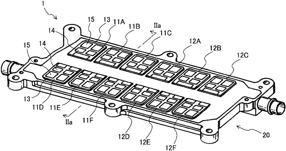
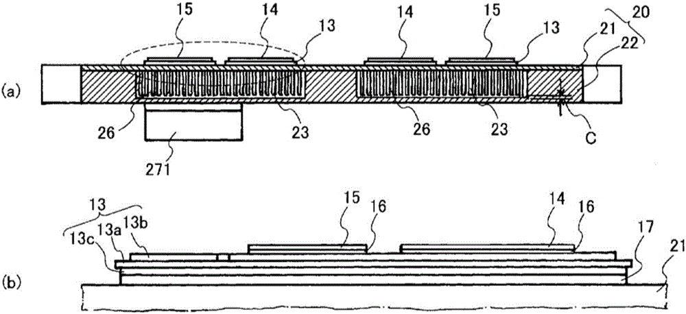
[0047] figure 1 It is a perspective view showing the appearance of an example of a semiconductor module which is an embodiment of the semiconductor device of the present invention. figure 2 (a) is represented by IIa-IIa line view section figure 1A schematic diagram of the semiconductor module, figure 2 (b) is figure 2 The enlarged partial schematic of (a).

[0048] Such as figure 1 with figure 2 As shown in (a) and (b), the semiconductor module 1 includes a plurality of circuit element units 11A to 11F, 12A to 12F and a cooler 20 connected to these circuit element units 11A to 11F, 12A to 12F.

[0049] Each of the circuit element portions 11A to 11F and 12A to 12F has a structure in which, for example, two semiconductor elements 14 and 15 of two types are mounted on the circuit board 13 , that is, a total of four semiconductor elements are mounted. Depend on figure 2 (b) shows that the circuit board 13 has a structure in which the conductive layers 13b and 13c a...

Embodiment approach 2

[0088] Next, a semiconductor device according to Embodiment 2 of the present invention will be described. The semiconductor device of the present embodiment has the same configuration as that of the semiconductor device of the first embodiment except for the shapes of the connection portion 271 and the connection portion 281 in the semiconductor device of the first embodiment. Therefore, the shapes of the connecting portion 271 and the connecting portion 281 will be described below. In addition, for the semiconductor device having the same description as the first embodiment, Figure 5 with Figure 7 Components described in and parts thereof with the same functions are denoted by the same reference numerals, and repeated descriptions are omitted below.

[0089] Figure 9 An enlarged view of the connection portion 271 of the semiconductor device according to Embodiment 2 is shown. and Figure 7 Compared with the first inclined surface 271a of the first embodiment shown, ...

Embodiment approach 3

[0093] Next, a semiconductor device according to Embodiment 3 of the present invention will be described. The semiconductor device of the present embodiment has the same structure as that of the semiconductor device of the first embodiment except for the structure of the cooling channel 26 in the semiconductor device of the first embodiment. Therefore, the structure of the cooling flow path 26 of this embodiment will be described below.

[0094] Figure 10 A plan view showing the internal structure of the cooler 20 in the semiconductor device of this embodiment is shown in . Figure 10 is the same as that of the cooler shown in Embodiment 1 Figure 5 Corresponding drawings, for the Figure 5 The same reference numerals are assigned to the same members as those shown, and thus repeated description of each member will be omitted.

[0095] Figure 10 The housing 22 shown differs from the others in the presence or absence of a partition 22c connected to the introduction path ...


PUM


Abstract

A cooler (20) for a semiconductor device is provided with: an introduction part (27) and a discharge part (28) for a cooling liquid; an introduction path (24); a discharge path (25); and a cooling flow path (26). The introduction path (24) and the discharge path (25) are provided with asymmetric planar shapes. A part (271) connecting the introduction path (24) and the introduction part (27) faces the cooling flow path (26) in a section directly below a plurality of circuit boards (13) arranged on the cooler (20). A part (281) connecting the discharge path (25) and the discharge part (28) faces the cooling flow path (26) in a section directly below a plurality of circuit boards (13) arranged on the cooler (20).

Description

technical field [0001] The present invention relates to a semiconductor device including a cooler through which a coolant for cooling semiconductor elements circulates. Background technique [0002] In equipment using electric motors such as hybrid vehicles and electric vehicles, power conversion devices are used for energy saving. Semiconductor modules are widely used in this power conversion device. This semiconductor module includes a power semiconductor element in order to control a large current. [0003] Power semiconductor components generate large amounts of heat when controlling large currents. In addition, since semiconductor modules are required to be miniaturized and lightweight, power density tends to increase. Therefore, in a semiconductor module including a plurality of power semiconductor elements, the cooling method affects power conversion efficiency. [0004] In order to improve the cooling efficiency of semiconductor modules, liquid-cooled coolers have...

Claims


Application Information

Patent Timeline
Patent Type & Authority Applications(China)
IPC IPC(8): H01L23/473H01L25/07H01L25/18H05K7/20
CPCH01L23/3672H01L23/473H01L24/29H01L24/32H01L24/45H01L24/48H01L24/73H01L25/072H01L25/18H01L2224/291H01L2224/32225H01L2224/45655H01L2224/48227H01L2224/73265H01L2924/13055H05K7/20927H01L2924/014H01L2924/00014H01L2924/00012H01L23/3675
Inventor 乡原广道两角朗市村武
Owner FUJI ELECTRIC CO LTD
Learn More