One-bit full adder based on Fin FETs

A full adder, the eleventh technology, applied in the direction of logic circuits with logic functions, etc., can solve the problems of increasing power consumption, increasing the path delay of high-order carry signal generation, increasing circuit area, delay and power consumption, etc.

Active Publication Date: 2016-09-21
NINGBO UNIV
View PDF3 Cites 2 Cited by
  • Summary
  • Abstract
  • Description
  • Claims
  • Application Information

AI Technical Summary

Problems solved by technology

The one-bit full adder uses static complementary logic to generate the sum signal and the high-order carry signal output. A large number of N-type FinFET tubes and P-type FinFET tubes are used in the sum signal generation path and the high-order carry signal generation path. The one-bit full adder It is composed of 28 FinFET tubes, which increases the circuit area, delay and power consumption of a full adder. In addition, the low-order carry signal input terminal is set closer to the sum signal output terminal and the high-order carry signal output terminal. Although It can speed up the operation speed of one-bit full adder to a certain extent, but it will cause one-bit adder to have a larger load capacitance, which will further increase power consumption and increase the delay of the high-order carry signal generation path, so that the one-bit full adder Larger circuit area, delay, power consumption, and power-delay product (PDP)

Method used


Image

  • One-bit full adder based on Fin FETs
  • One-bit full adder based on Fin FETs
  • One-bit full adder based on Fin FETs

Examples


Embodiment 1

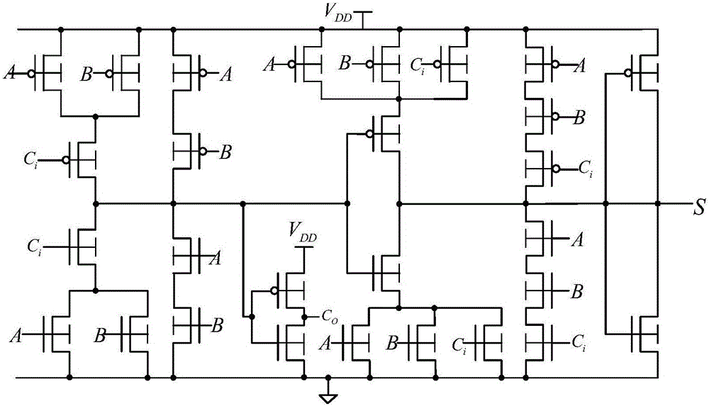
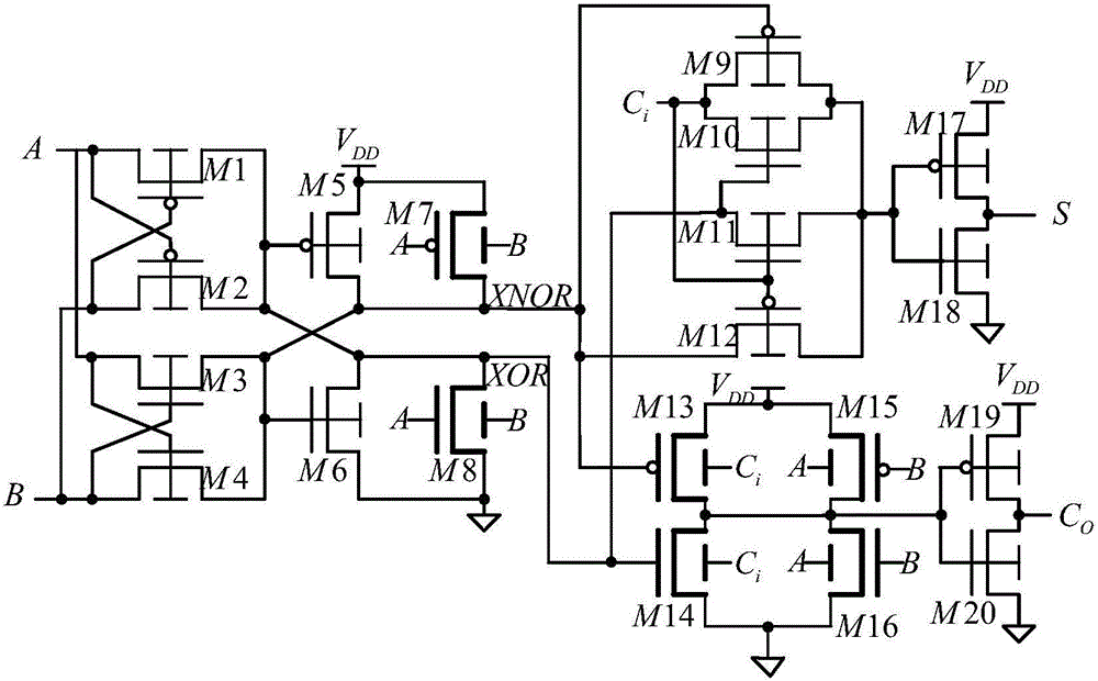
[0013] Embodiment one: if figure 2 As shown, a one-bit full adder based on FinFET tubes includes a first FinFET tube M1, a second FinFET tube M2, a third FinFET tube M3, a fourth FinFET tube M4, a fifth FinFET tube M5, and a sixth FinFET tube M6, the seventh FinFET tube M7, the eighth FinFET tube M8, the ninth FinFET tube M9, the tenth FinFET tube M10, the eleventh FinFET tube M11, the twelfth FinFET tube M12, the thirteenth FinFET tube M13, the fourteenth FinFET tube M14, fifteenth FinFET tube M15, sixteenth FinFET tube M16, seventeenth FinFET tube M17, eighteenth FinFET tube M18, nineteenth FinFET tube M19, twentieth FinFET tube M20, first FinFET tube M1, the second FinFET tube M2, the fifth FinFET tube M5, the seventh FinFET tube M7, the ninth FinFET tube M9, the twelfth FinFET tube M12, the thirteenth FinFET tube M13, the fifteenth FinFET tube M15, the seventeenth The FinFET tube M17 and the nineteenth FinFET tube M19 are P-type FinFET tubes, the third FinFET tube M3, th...

Embodiment 2

[0014] Embodiment two: if figure 2As shown, a one-bit full adder based on FinFET tubes includes a first FinFET tube M1, a second FinFET tube M2, a third FinFET tube M3, a fourth FinFET tube M4, a fifth FinFET tube M5, and a sixth FinFET tube M6, the seventh FinFET tube M7, the eighth FinFET tube M8, the ninth FinFET tube M9, the tenth FinFET tube M10, the eleventh FinFET tube M11, the twelfth FinFET tube M12, the thirteenth FinFET tube M13, the fourteenth FinFET tube M14, fifteenth FinFET tube M15, sixteenth FinFET tube M16, seventeenth FinFET tube M17, eighteenth FinFET tube M18, nineteenth FinFET tube M19, twentieth FinFET tube M20, first FinFET tube M1, the second FinFET tube M2, the fifth FinFET tube M5, the seventh FinFET tube M7, the ninth FinFET tube M9, the twelfth FinFET tube M12, the thirteenth FinFET tube M13, the fifteenth FinFET tube M15, the seventeenth The FinFET tube M17 and the nineteenth FinFET tube M19 are P-type FinFET tubes, the third FinFET tube M3, the...


PUM


Abstract

The invention discloses a one-bit full adder based on Fin FETs. The one-bit full adder comprises first to twenty Fin FETs. The first Fin FET, the second Fin FET, the fifth Fin FET, the seventh Fin FET, the ninth Fin FET, the twelfth Fin FET, the thirteenth Fin FET, the fifteenth Fin FET, the seventeenth Fin FET, and the nineteenth Fin FET are P-type Fin FETs. The third Fin FET, the fourth Fin FET, the sixth Fin FET, the eighth Fin FET, the tenth Fin FET, the eleventh Fin FET, the fourteenth Fin FET, the sixteenth Fin FET, the eighteenth Fin FET, and the twentieth Fin FET are N-type Fin FETs. The one-bit full adder is low in circuit area, time delay, power consumption, and power consumption time delay product.

Description

technical field [0001] The invention relates to a one-bit full adder, in particular to a one-bit full adder based on a FinFET tube. Background technique [0002] As a basic unit of an electronic system, a full adder can not only complete addition, but also participate in operations such as subtraction, multiplication, and division, and is widely used in large-scale integrated circuit design. The full adder is an important unit of a digital signal processor, a microprocessor, and a single-chip microcomputer system with relatively high performance requirements. The performance of the full adder has a particularly important impact on the performance of the entire system. One-bit full adder is widely used in the carry critical path of multi-bit adder, and is one of the important factors affecting multi-bit adder. FinFET tube (Fin Field-Effect Transistor, Fin Field-Effect Transistor) is a complementary metal oxide semiconductor (CMOS) transistor, which has the advantages of high...

Claims


Application Information

Patent Timeline
Patent Type & Authority Applications(China)
IPC IPC(8): H03K19/20
CPCH03K19/20
Inventor 胡建平许仲池
Owner NINGBO UNIV
Why Eureka
Try Eureka