Calibration method and device for transmitter chip

A calibration method and calibration device technology, applied in transmitter monitoring and other directions, can solve the problems of increasing test cost, difficulty in improving calibration and test efficiency, and inability to test multiple chips at the same time, so as to save costs and improve test efficiency Effect

Inactive Publication Date: 2016-09-21
BEIJING WINNER MICROELECTRONICS
View PDF6 Cites 2 Cited by
  • Summary
  • Abstract
  • Description
  • Claims
  • Application Information

AI Technical Summary

Problems solved by technology

This method requires additional instrumentation, increasing the cost of testing
At the same time, one instrument can only correspond to one RF chip. If you do not purchase multiple instruments, it is impossible to test multiple chips at the same time, and it is difficult to improve the efficiency of calibration and testing.

Method used


Image

  • Calibration method and device for transmitter chip
  • Calibration method and device for transmitter chip
  • Calibration method and device for transmitter chip

Examples


Embodiment 1

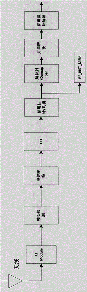
[0046] Based on the requirements of the communication system for cost, area, power consumption and integration, the zero-IF transceiver has a simpler structure, higher bandwidth, smaller area and lower power consumption than the superheterodyne transceiver. It is widely used in communication systems. But because of its relatively simple structure, it is more susceptible to various noise pollution. For example, the DC bias will lead to signal degradation and saturation of the receiver stage, while the amplitude or phase imbalance of the in-phase I / quadrature Q two channels will lead to the deterioration of the demodulated signal constellation. Therefore, for WIFI RF chips, using algorithms to calibrate the DC bias and I / Q imbalance will greatly improve the performance of the RF circuit.

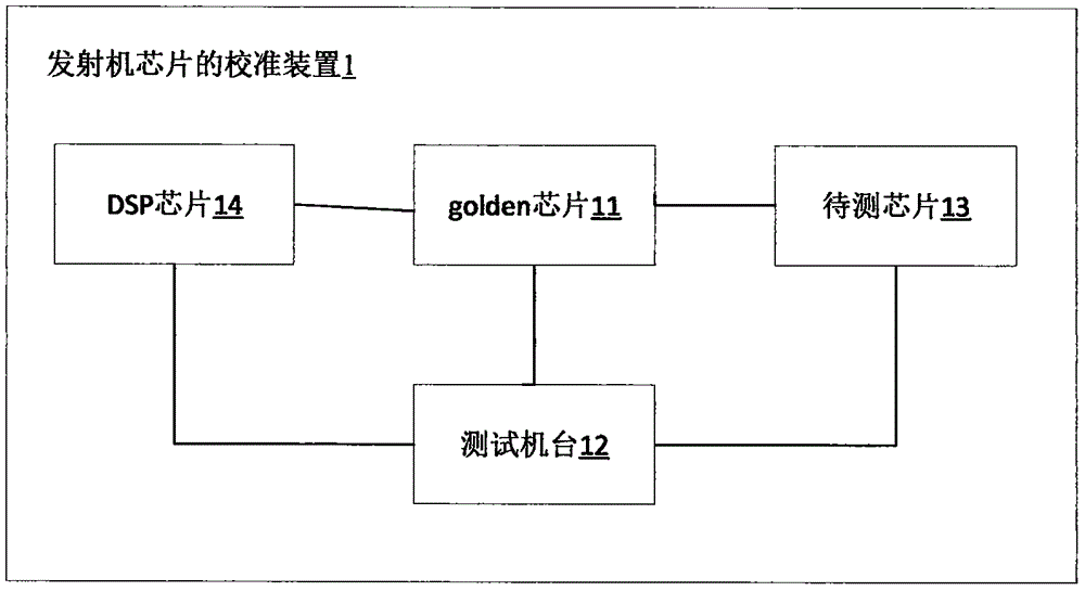
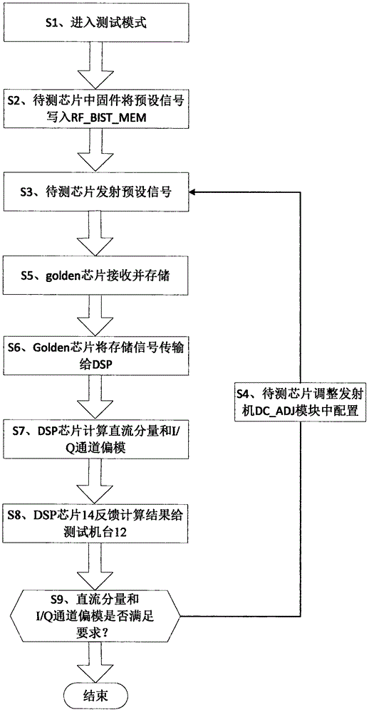
[0047] figure 1 A schematic structural diagram showing a calibration device for a transmitter chip provided by an embodiment of the present invention, as shown in figure 1 As shown, the c...


PUM


Abstract

The present invention relates to a calibration method and device for a transmitter chip. The method comprises the steps that a chip to be tested transmits a sinusoidal signal to a standard chip such that the standard chip can transmit the sinusoidal signal to a digital signal processing chip for analysis; the chip to be tested adjusts a DC bias parameter and an I/Q channel bias mode parameter according to the testing result sent by a testing machine platform, wherein the testing result sent by the testing machine platform is obtained by analyzing the sinusoidal signal by the digital signal processing chip. According to the calibration method and device for a transmitter chip provided by the invention, the chip can be used to transmit and receive the signal of the chip to be tested and carry out analyzing, the instrument in a conventional calibration and test mode is replaced, and the automation of calibration and test is realized through a firmware.

Description

technical field [0001] The invention relates to the field of WIFI chips for the Internet of Things, in particular to a calibration method and device for a transmitter chip. Background technique [0002] Due to the difference of devices in the chip manufacturing process and the influence of temperature and external environment on the operation of the internal devices of the chip, even the RF chips produced in the same batch will have certain differences in performance. In order to ensure the consistency of the product, before the product is delivered, the analog circuit of the WIFI RF chip will be calibrated with DC bias, in-phase I / quadrature Q two-way phase and amplitude, to correct the analog circuit due to the process deviation in the manufacturing process. The impact of work, and performance testing will also be carried out to ensure that the delivered products meet the performance requirements. [0003] Generally, when calibrating and testing radio frequency chips, spe...

Claims


Application Information

Patent Timeline
Patent Type & Authority Applications(China)
IPC IPC(8): H04B17/11
CPCH04B17/11
Inventor 梅张雄程晟
Owner BEIJING WINNER MICROELECTRONICS
Why Eureka
Try Eureka