An adiabatic pal-2n jk flip-flop based on finfet device

A PAL-2N, structural technology, applied in electrical components, pulse technology, pulse generation, etc., can solve the problem of energy can not be released or recovered, energy loss, circuit area, delay, power consumption and power consumption delay product And other issues

Active Publication Date: 2018-10-09
NINGBO UNIV
View PDF3 Cites 0 Cited by
  • Summary
  • Abstract
  • Description
  • Claims
  • Application Information

AI Technical Summary

Problems solved by technology

[0004] However, the existing JK flip-flop based on the adiabatic ECRL structure of FinFET devices has the following problems: the existing JK flip-flop based on the adiabatic ECRL structure of FinFET devices uses 22 FinFET tubes to realize the JK flip-flop function, and the number of FinFET tubes is large. Moreover, due to the existence of the threshold voltage of the P-type FinFET tube contained in it, the energy cannot be fully released or recovered in the pre-charging stage and the evaluation stage, and part of the energy is consumed in the resistance, which is lost in the form of heat energy, and its output The node suspension will cause a certain energy loss, which leads to the existing FinFET-based adiabatic ECRL structure type JK flip-flop circuit area, delay, power consumption and power consumption delay product are large

Method used


Image

  • An adiabatic pal-2n jk flip-flop based on finfet device
  • An adiabatic pal-2n jk flip-flop based on finfet device
  • An adiabatic pal-2n jk flip-flop based on finfet device

Examples


Embodiment 1

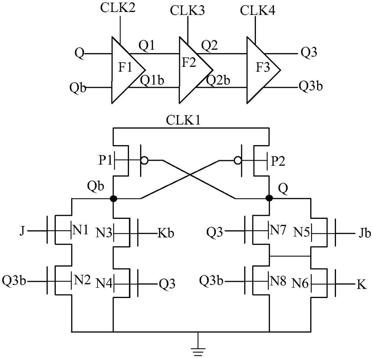
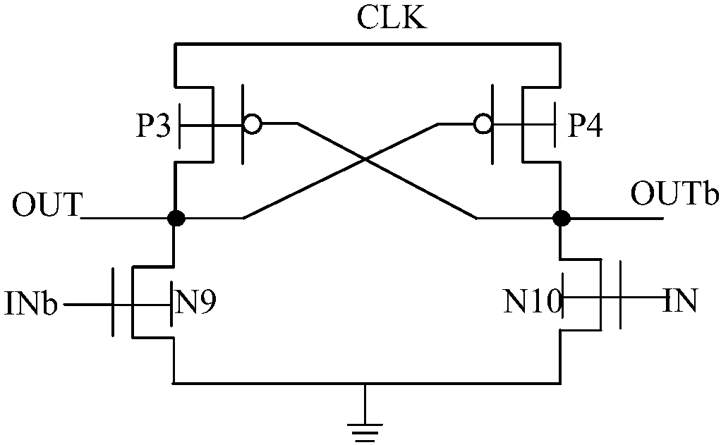
[0024] Embodiment one: if Figure 4 As shown, a JK flip-flop based on FinFET device adiabatic PAL-2N structure includes the first P-type FinFET tube P1, the second P-type FinFET tube P2, the third P-type FinFET tube P3, and the fourth P-type FinFET tube P4 , the first N-type FinFET tube N1, the second N-type FinFET tube N2, the third N-type FinFET tube N3, the fourth N-type FinFET tube N4, the fifth N-type FinFET tube N5, the sixth N-type FinFET tube N6, the The seventh N-type FinFET tube N7, the eighth N-type FinFET tube N8, the ninth N-type FinFET tube N9, the tenth N-type FinFET tube N10, and the eleventh N-type FinFET tube N11; the source of the first P-type FinFET tube P1 , the source of the second P-type FinFET transistor P2, the source electrode of the third N-type FinFET transistor N3, the source electrode of the fourth N-type FinFET transistor N4, the source electrode of the fifth N-type FinFET transistor N5, the sixth N-type FinFET transistor The source of the tube ...

Embodiment 2

[0026] Embodiment two: if Figure 4 As shown, a JK flip-flop based on FinFET device adiabatic PAL-2N structure includes the first P-type FinFET tube P1, the second P-type FinFET tube P2, the third P-type FinFET tube P3, and the fourth P-type FinFET tube P4 , the first N-type FinFET tube N1, the second N-type FinFET tube N2, the third N-type FinFET tube N3, the fourth N-type FinFET tube N4, the fifth N-type FinFET tube N5, the sixth N-type FinFET tube N6, the The seventh N-type FinFET tube N7, the eighth N-type FinFET tube N8, the ninth N-type FinFET tube N9, the tenth N-type FinFET tube N10, and the eleventh N-type FinFET tube N11; the source of the first P-type FinFET tube P1 , the source of the second P-type FinFET transistor P2, the source electrode of the third N-type FinFET transistor N3, the source electrode of the fourth N-type FinFET transistor N4, the source electrode of the fifth N-type FinFET transistor N5, the sixth N-type FinFET transistor The source of the tube ...

Embodiment 3

[0029] Embodiment three: as Figure 4 As shown, a JK flip-flop based on FinFET device adiabatic PAL-2N structure includes the first P-type FinFET tube P1, the second P-type FinFET tube P2, the third P-type FinFET tube P3, and the fourth P-type FinFET tube P4 , the first N-type FinFET tube N1, the second N-type FinFET tube N2, the third N-type FinFET tube N3, the fourth N-type FinFET tube N4, the fifth N-type FinFET tube N5, the sixth N-type FinFET tube N6, the The seventh N-type FinFET tube N7, the eighth N-type FinFET tube N8, the ninth N-type FinFET tube N9, the tenth N-type FinFET tube N10, and the eleventh N-type FinFET tube N11; the source of the first P-type FinFET tube P1 , the source of the second P-type FinFET transistor P2, the source electrode of the third N-type FinFET transistor N3, the source electrode of the fourth N-type FinFET transistor N4, the source electrode of the fifth N-type FinFET transistor N5, the sixth N-type FinFET transistor The source of the tub...


PUM


Abstract

The invention discloses an adiabatic PAL-2N structure type JK flip-flop based on Fin-FET devices, comprising a first P-type Fin-FET, a second P-type Fin-FET, a third P-type Fin-FET, a fourth P-type Fin-FET, a first N-type Fin-FET, a second N-type Fin-FET, a third N-type Fin-FET, a fourth N-type Fin-FET, a fifth N-type Fin-FET, a sixth N-type Fin-FET, a seventh N-type Fin-FET, an eighth N-type Fin-FET, a ninth N-type Fin-FET, a tenth N-type Fin-FET and an eleventh N-type Fin-FET. The advantage is that under the condition that the circuit performance of the adiabatic PAL-2N structure type JK flip-flop is not affected, the number of Fin-FETs is reduced, the circuit area is reduced significantly, and the time delay, power consumption and power-delay product are reduced significantly.

Description

technical field [0001] The invention relates to a JK flip-flop based on a FinFET device, in particular to an adiabatic PAL-2N structure type JK flip-flop based on a FinFET device. Background technique [0002] The JK flip-flop is an indispensable basic sequential circuit in the digital circuit system, and has an important position in the digital circuit system. The adiabatic ECRL circuit adopts the differential structure of double input and double output. The existing JK flip-flop with better performance is usually realized by the ECRL circuit structure. At present, we call the JK flip-flop realized by the adiabatic ECRL circuit structure as the adiabatic ECRL structure type JK trigger. [0003] With the continuous advancement of VISL technology, the operating speed of digital circuit systems is constantly increasing, and the requirements for the speed of JK flip-flops are also getting higher and higher. FinFET tube (Fin Field-Effect Transistor, Fin Field-Effect Transistor...

Claims


Application Information

Patent Timeline
Patent Type & Authority Patents(China)
IPC IPC(8): H03K3/012
CPCH03K3/012
Inventor 胡建平余峰
Owner NINGBO UNIV
Why Eureka
Try Eureka