Optical image capture system, image capture device and electronic device

An optical imaging system, image-side technology, applied in optics, optical components, instruments, etc., can solve problems such as inability to demonstrate imaging effects, inability to meet photography systems, and too dark around the image.

Active Publication Date: 2016-10-05
LARGAN PRECISION
View PDF9 Cites 25 Cited by
  • Summary
  • Abstract
  • Description
  • Claims
  • Application Information

AI Technical Summary

Problems solved by technology

[0003] Traditionally, optical systems mounted on electronic products mostly use four-element or five-element lens structures. However, due to the prevalence of high-standard mobile devices such as smart phones (Smart Phone) and tablet computers (Tablet PC), the optical system is driven by the pixel With the rapid increase in imaging quality, known optical systems will not be able to meet higher-level photographic systems
Moreover, the resolution of the optical system traditionally configured in the vehicle camera device is relatively insufficient, but due

Method used


Image

  • Optical image capture system, image capture device and electronic device
  • Optical image capture system, image capture device and electronic device
  • Optical image capture system, image capture device and electronic device

Examples


no. 1 example

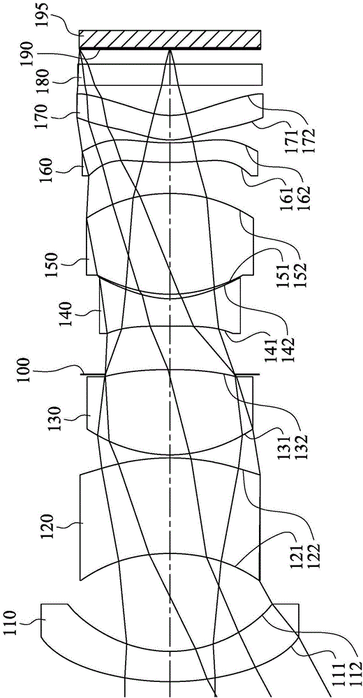
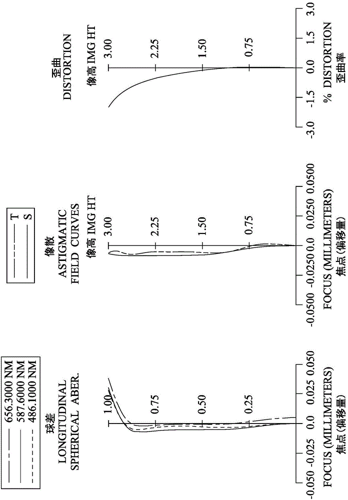
[0121] Please refer to figure 1 and figure 2 ,in figure 1 A schematic diagram showing an imaging device according to the first embodiment of the present invention, figure 2 From left to right are the spherical aberration, astigmatism and distortion curves of the first embodiment. Depend on figure 1 It can be seen that the imaging device of the first embodiment includes an optical imaging system (not labeled separately) and an electronic photosensitive element 195 . The optical imaging system includes a first lens 110, a second lens 120, a third lens 130, an aperture 100, a fourth lens 140, a fifth lens 150, a sixth lens 160, and a seventh lens 170 from the object side to the image side in sequence , the infrared filter element 180 and the imaging surface 190, and the electronic photosensitive element 195 is arranged on the imaging surface 190 of the optical imaging system, wherein there are seven lenses (110-170) with refractive power in the optical imaging system, and ...

no. 2 example

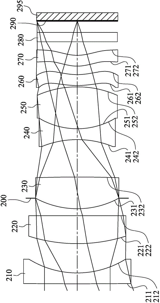
[0157] Please refer to image 3 and Figure 4 ,in image 3 A schematic diagram showing an imaging device according to a second embodiment of the present invention, Figure 4 From left to right are the spherical aberration, astigmatism and distortion curves of the second embodiment. Depend on image 3 It can be seen that the imaging device of the second embodiment includes an optical imaging system (not labeled separately) and an electronic photosensitive element 295 . The optical imaging system includes a first lens 210, a second lens 220, an aperture 200, a third lens 230, a fourth lens 240, a fifth lens 250, a sixth lens 260, and a seventh lens 270 from the object side to the image side. , the infrared filter filter element 280 and the imaging surface 290, and the electronic photosensitive element 295 is arranged on the imaging surface 290 of the optical imaging system, wherein there are seven lenses (210-270) with refractive power in the optical imaging system, and The...

no. 3 example

[0174] Please refer to Figure 5 and Figure 6 ,in Figure 5 A schematic diagram showing an imaging device according to a third embodiment of the present invention, Figure 6 From left to right are the spherical aberration, astigmatism and distortion curves of the third embodiment. Depend on Figure 5 It can be seen that the imaging device of the third embodiment includes an optical imaging system (not labeled separately) and an electronic photosensitive element 395 . The optical imaging system includes a first lens 310, a second lens 320, an aperture 300, a third lens 330, a fourth lens 340, a fifth lens 350, a sixth lens 360, and a seventh lens 370 from the object side to the image side in sequence , the infrared filter element 380 and the imaging surface 390, and the electronic photosensitive element 395 is arranged on the imaging surface 390 of the optical imaging system, wherein there are seven lenses (310-370) with refractive power in the optical imaging system, and ...


PUM


Abstract

The invention discloses an optical image capture system, an image capture device and an electronic device. The optical image capture system comprises a first lens, a second lens, a third lens, a fourth lens, a fifth lens, a sixth lens and a seventh lens in sequence from an object side to an image side. The first lens has negative refractive power, and the image-side surface is concave near the optical axis. The second lens has refractive power. The third lens has refractive power. The fourth lens has refractive power. The fifth lens has refractive power. The sixth lens has refractive power, the image-side surface is concave near the optical axis and contains at least one convex surface away from the optical axis, and both the object-side surface and the image-side surface are aspheric surfaces. The seventh lens has refractive power, the image-side surface is concave near the optical axis and contains at least one convex surface away from the optical axis, and both the object-side surface and the image-side surface are aspheric surfaces. When certain conditions are met, aberration is avoided. The invention further discloses an image capture device comprising the optical image capture system and an electronic device comprising the image capture device.

Description

technical field [0001] The invention relates to an optical image pickup system and an image pickup device, and in particular to a miniaturized optical image pickup system and an image pickup device applied to electronic devices. Background technique [0002] In recent years, with the rise of electronic products with photographic functions, the demand for optical systems has increased day by day. The photosensitive element of the general optical system is nothing more than two types of photosensitive coupling device (Charge Coupled Device, CCD) or complementary metal oxide semiconductor element (Complementary Metal-Oxide Semiconductor Sensor, CMOS Sensor), and with the advancement of semiconductor technology, making The pixel size of the photosensitive element is shrinking, and the optical system is gradually developing into the high-pixel field, so the requirements for image quality are also increasing. [0003] Traditionally, optical systems mounted on electronic products ...

Claims


Application Information

Patent Timeline
IPC IPC(8): G02B13/18G02B13/00
Inventor 廖凌峣谢东益陈纬彧
Owner LARGAN PRECISION
Why Eureka
Try Eureka