Semiconductor structures and methods of forming them
A semiconductor and gate structure technology, which is applied in the field of semiconductor structures and their formation, can solve problems such as poor performance of semiconductor structures, and achieve the goals of improving yield, reducing mismatch probability, and reducing threshold voltage floating difference and probability Effect
- Summary
- Abstract
- Description
- Claims
- Application Information
AI Technical Summary
Problems solved by technology
Method used
Image

Examples
Embodiment 1
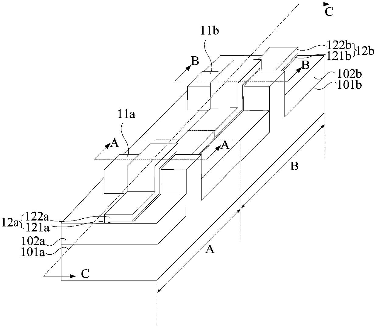
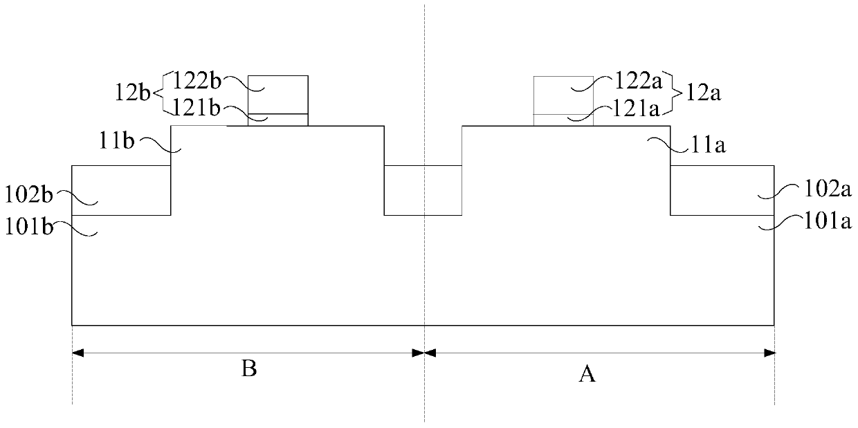
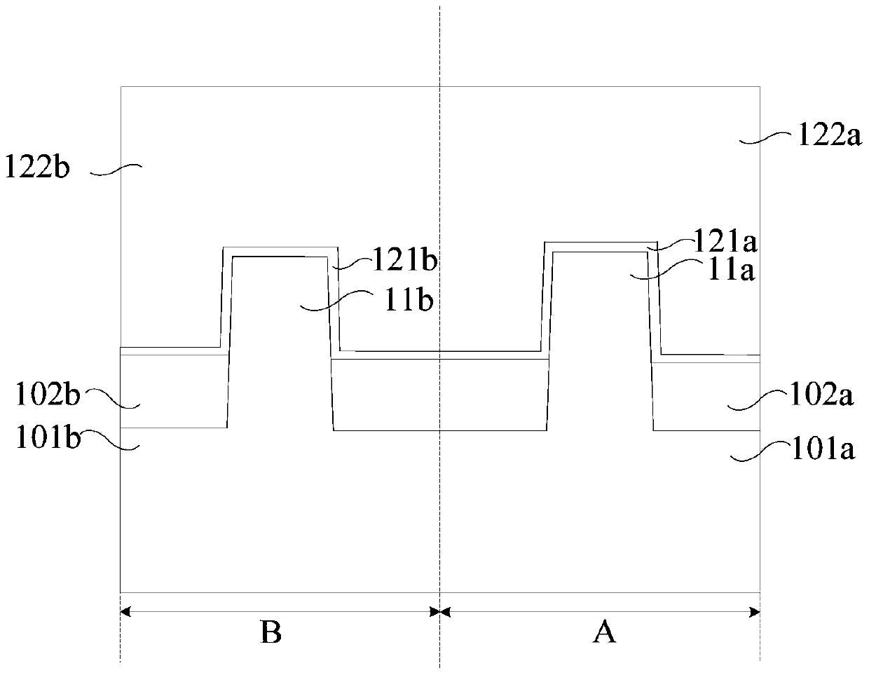
[0078] First, combine the reference Figure 14 (a), 15(a) and 16(a), provide a semiconductor substrate, the semiconductor substrate includes an SRAM area I, the SRAM area I includes a first PMOS area A and a first NMOS area B, and the second A PMOS region A has a first fin 31a, and the first NMOS region B has a second fin 31b. The specific formation method is as follows:
[0079] The semiconductor substrate of the first PMOS region A includes a silicon substrate 301a having at least two discrete raised structures and an insulating layer 302a between the raised structures, the insulating layer 302a being lower than the raised structures. The raised structure higher than the insulating layer 302a is the first fin 31a.
[0080] The semiconductor substrate of the first NMOS region B includes a silicon substrate 301b having at least two discrete raised structures and an insulating layer 302b between the raised structures, the insulating layer 302b being lower than the raised stru...
Embodiment 2
[0133] The difference between embodiment two and embodiment one is:
[0134] combined reference Figure 14 to Figure 16 , the semiconductor substrate in Embodiment 1 further includes a logic region II, the logic region includes a second PMOS region C and a second NMOS region D, the second PMOS region C has a third fin 41a, and the second The NMOS region D has a fourth fin 41b.
[0135] The specific formation method is as follows:
[0136] The semiconductor substrate of the second PMOS region C includes a silicon substrate 401a having at least two discrete raised structures and an insulating layer 402a between the raised structures, the insulating layer 402a being lower than the raised structures 402a. The raised structure higher than the insulating layer 402a is the third fin 41a.
[0137] The semiconductor substrate in the second NMOS region D includes a silicon substrate 401b having at least two discrete raised structures and an insulating layer 402b between the raised stru...
Embodiment 3
[0195] The present invention provides a semiconductor structure, with reference to Figure 33 (a) and Figure 34 (a), including:
[0196] A semiconductor substrate having a SRAM region I comprising a first PMOS region A having a first fin 31a and a first NMOS region B having a first NMOS region B having a first fin 31a. two fins 31b;
[0197] a first gate structure across the first fin 31a, the first gate structure having a first work function layer;
[0198] a second gate structure across the second fin 31b, the second gate structure having a second work function layer;
[0199] The materials of the first work function layer and the second work function layer are the same.
[0200] In this embodiment, the first work function layer is a stack of the first work function material layer 81 on the bottom and the second work function material layer 82 on the top, or the second work function material layer 82, and the first work function material layer The material of the layer...
PUM
 Abstract
Description
Claims
Application Information
 - R&D
- Intellectual Property
- Life Sciences
- Materials
- Tech Scout
- Unparalleled Data Quality
- Higher Quality Content
- 60% Fewer Hallucinations
Browse by: Latest US Patents, China's latest patents, Technical Efficacy Thesaurus, Application Domain, Technology Topic, Popular Technical Reports.
© 2025 PatSnap. All rights reserved.Legal|Privacy policy|Modern Slavery Act Transparency Statement|Sitemap|About US| Contact US: help@patsnap.com