Line recognition and display device

A display device, texture technology, applied in radiation control devices, character and pattern recognition, circuits, etc., can solve problems such as large divergence angle, optical crosstalk, diffuse reflection, etc.

Active Publication Date: 2016-10-12
BOE TECH GRP CO LTD
View PDF6 Cites 90 Cited by
  • Summary
  • Abstract
  • Description
  • Claims
  • Application Information

AI Technical Summary

Problems solved by technology

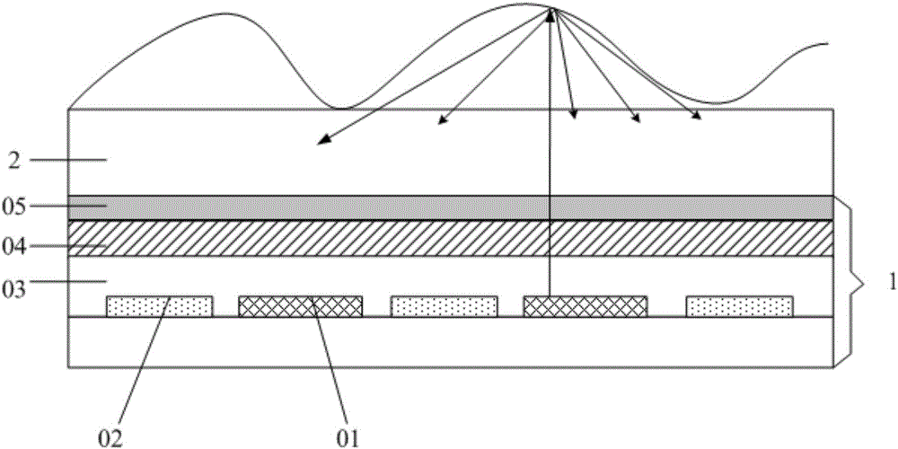
But in the above-mentioned fingerprint identification display device, such as figure 1 As shown, when a finger presses the protective cover 2, at least the packaging film 03 of the display panel 1, the polarizer layer 04, the transparent optical adhesive layer 05 and the protective cover 2 are arranged between the photosensitive unit 02 and the finger. The distance between the finger and the photosensitive unit 02 is relatively long, and the light emitted by the organic electroluminescent pixel unit 01 will form diffuse reflection when it passes through these film l

Method used


Image

  • Line recognition and display device
  • Line recognition and display device
  • Line recognition and display device

Examples


Embodiment 1

[0073] In the above-mentioned texture recognition and display device provided by the embodiment of the present invention, such as Figure 7aAs shown, it includes: an array substrate 10, a gate 30 sequentially located on the array substrate 10, a gate insulating layer 31, an active layer 32, a first dielectric layer 33, a reference signal line 18, and a second dielectric layer 34, which are arranged in the same layer. The source electrode 35 and the drain electrode 36, the first insulating layer 37, the identification output line 17 arranged on the same layer, the first connecting part 38 and the second connecting part 39, the photosensitive unit 12, the second insulating layer 40, arranged on the same layer The first electrode layer 111a, the third connecting portion 41 and the light shielding portion 14, the pixel defining layer 42, the light emitting layer 111b, the second electrode layer 111c, the packaging film 43, the condenser lens 13, the polarizing layer 44, the transpa...

Embodiment 2

[0079] In the above-mentioned texture recognition and display device provided by the embodiment of the present invention, such as Figure 7b As shown, it includes: an array substrate 10, a gate 30 sequentially located on the array substrate 10, a gate insulating layer 31, an active layer 32, a first dielectric layer 33, a reference signal line 18, and a second dielectric layer 34, which are arranged in the same layer. The source electrode 35 and the drain electrode 36, the first insulating layer 37, the identification output line 17 arranged on the same layer, the first connecting part 38 and the second connecting part 39, the photosensitive unit 12, the second insulating layer 40, arranged on the same layer The first electrode layer 111a and the third connection part 41, the first pixel definition layer 42, the light shielding part 14, the second pixel definition layer 43, the light emitting layer 111b, the second electrode layer 111c, the encapsulation film 44, the condenser ...


PUM


Abstract

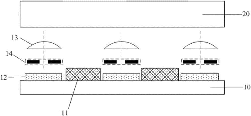
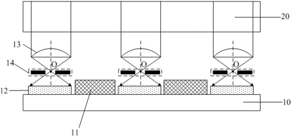
The invention discloses a line recognition and display device. The device comprises an array substrate, a line bearing plate opposite to the array substrate, light-sensing units, condensing lenses and shading parts, wherein the light-sensing units in at least part of pixel areas are located on the array substrate, the condensing lenses correspond to the light-sensing unit one to one and are located at the sides, facing the line bearing plate, of the light-sensing units, and the shading parts correspond to the condensing lenses one to one and are located between the condensing lenses and the corresponding light-sensing units. When a finger or palm makes contact with the line bearing plate, light which is reflected by the finger or palm and irradiated to the condensing lenses is gathered in the main optical axis direction by means of the condensing lenses, but only part of light meeting specific conditions can irradiate to the light-sensing units because of light-pervious holes, and accordingly the light-sensing units only collect light in the specific transmission direction. Thus, no matter how far the light-sensing units are from the upper surface of the line bearing plate, optical crosstalk can be reduced.

Description

technical field [0001] The invention relates to the field of display technology, in particular to a texture recognition display device. Background technique [0002] With the rapid development of display technology, touch screen panels (Touch Screen Panels) have gradually spread in people's lives. At present, touch screens can be divided into: resistive, capacitive, infrared, surface acoustic wave, electromagnetic, vibration induction, and frustrated total internal reflection optical induction, etc. according to their working principles. [0003] And in the personal verification system based on security of the touch screen, the method of using fingerprints for identification has been widely used. At present, existing fingerprint identification display devices such as figure 1 As shown, it mainly includes a display panel 1 and a protective cover 2 located on the display panel 1; wherein the display panel 1 has pixel areas arranged in a matrix, and each pixel area is provide...

Claims


Application Information

Patent Timeline
IPC IPC(8): G06K9/00
CPCG06V40/1324G06V40/12H01L27/14678G06V40/1318H01L27/146G06F18/00
Inventor 吴俊纬董学王海生刘英明丁小梁吕敬
Owner BOE TECH GRP CO LTD
Why Eureka
Try Eureka