Trench Schottky chip applicable to metal wire bonding and processing technology thereof

A metal wire and bonding technology, applied to electrical components, electrical solid devices, circuits, etc., can solve problems such as chip failure and groove damage, and achieve the effects of improving chip performance, reducing consumption, and facilitating finding fault points

Active Publication Date: 2016-10-12
YANGZHOU YANGJIE ELECTRONIC TECH CO LTD
View PDF6 Cites 1 Cited by
  • Summary
  • Abstract
  • Description
  • Claims
  • Application Information

AI Technical Summary

Problems solved by technology

However, since wire bonding and packaging are performed directly on the surface of the groove, groove damage is prone to occur during wire bonding and packaging, resulting in chip failure

Method used


Image

  • Trench Schottky chip applicable to metal wire bonding and processing technology thereof
  • Trench Schottky chip applicable to metal wire bonding and processing technology thereof
  • Trench Schottky chip applicable to metal wire bonding and processing technology thereof

Examples


Embodiment 1

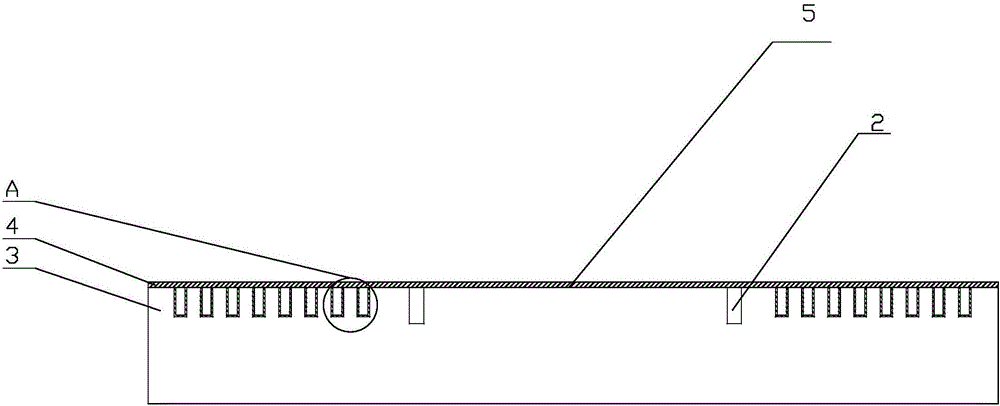
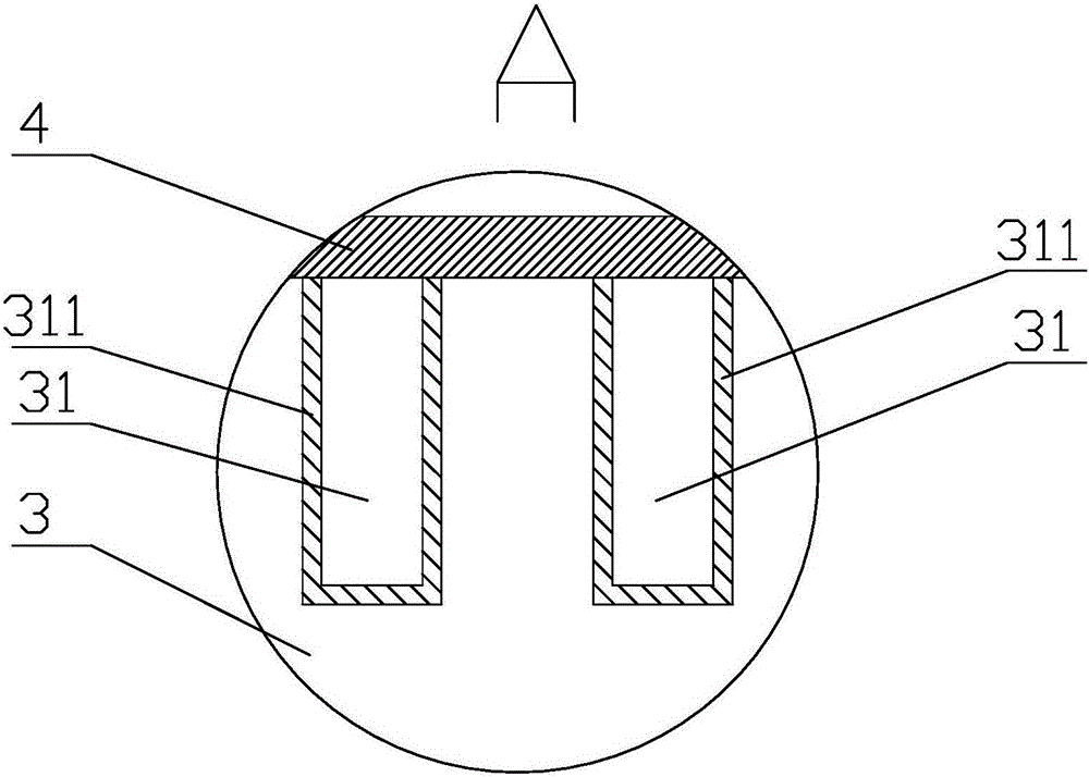
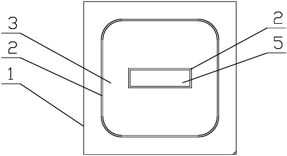
[0036] Such as image 3 As shown, an oxide layer is provided around the trench area to avoid chip damage during processing. The trench region 3 is evenly distributed with grooves 31, and the grooves 31 are filled with polysilicon material, which is used to increase the contact area of ​​the chip and reduce the forward conduction voltage, and obtain a lower reverse voltage by selecting a barrier metal with a higher energy level. to the leakage current. Surface metal is laid on the surface of the trench area. Use the good electrical conductivity of the surface metal to conduct with the plane bonding area. The trench area 3 is also provided with a plane bonding area 5 , the plane bonding area 5 is a smooth plane, and the surface metal 4 is laid on the plane bonding area 5 . The surface metal 4 has good electrical conductivity, which reduces the internal resistance of the chip, thereby reducing power consumption of the chip. The planar bonding area 5 is used for soldering with...

Embodiment 2

[0038] Such as Figure 4As shown, an oxide layer is provided around the trench area to avoid chip damage during processing. The trench region 3 is evenly distributed with grooves 31, and the grooves 31 are filled with polysilicon material, which is used to increase the contact area of ​​the chip and reduce the forward conduction voltage, and obtain a lower reverse voltage by selecting a barrier metal with a higher energy level. to the leakage current. Surface metal is laid on the surface of the trench area. Use the good electrical conductivity of the surface metal to conduct with the plane bonding area. The trench area 3 is also provided with a plane bonding area 5 , the plane bonding area 5 is a smooth plane, and the surface metal 4 is laid on the plane bonding area 5 . The surface metal 4 has good electrical conductivity, which reduces the internal resistance of the chip, thereby reducing power consumption of the chip. The planar bonding area 5 is used for soldering with...

Embodiment 3

[0040] Such as Figure 5 As shown, an oxide layer is provided around the trench area to avoid chip damage during processing. The trench region 3 is evenly distributed with grooves 31, and the grooves 31 are filled with polysilicon material, which is used to increase the contact area of ​​the chip and reduce the forward conduction voltage, and obtain a lower reverse voltage by selecting a barrier metal with a higher energy level. to the leakage current. Surface metal is laid on the surface of the trench area. Use the good electrical conductivity of the surface metal to conduct with the plane bonding area. The trench area 3 is also provided with a plane bonding area 5 , the plane bonding area 5 is a smooth plane, and the surface metal 4 is laid on the plane bonding area 5 . The surface metal 4 has good electrical conductivity, which reduces the internal resistance of the chip, thereby reducing power consumption of the chip. The planar bonding area 5 is used for soldering wit...


PUM


Abstract

The invention relates to a Schottky chip and a processing technology thereof, particularly relates to a Schottky chip applicable to metal wire bonding and a processing technology thereof, and provides a trench Schottky chip applicable to metal wire bonding which is additionally provided with a plane bonding region in a chip area so as to avoid trench damages and a processing technology thereof. The trench region is further provided with a plane bonding region, wherein the plane bonding region is a smooth plane, and the plane bonding region is laid with surface metal. The edge of the trench region and the edge of the plane bonding region are respectively provided with protection rings. The inner wall of the trench is subjected to oxidation treatment so as to form a silicon dioxide layer. The trench Schottky chip applicable to metal wire bonding and the processing technology thereof are convenient for a user to use, and also facilitate a producer to differentiate the bonding line trend, thereby enabling chip connection to be more visual, and being convenient for locating a fault point.

Description

technical field [0001] The invention relates to a Schottky chip and its processing technology, in particular to a Schottky chip suitable for wire bonding and its processing technology. Background technique [0002] At present, the Schottky of the traditional planar barrier technology has the problem of mutual limitation of reverse leakage current and forward conduction voltage. Choosing different barrier metals will lead to two limitations. One is that there is a higher reverse leakage current. And lower forward conduction voltage, this situation will produce reverse power consumption in the load process, the second is lower reverse leakage and higher forward conduction voltage, higher forward conduction voltage, will produce load The forward power consumption of the process. Both higher reverse power consumption and higher forward power consumption will reduce the conversion efficiency, or cause the device to fail when the junction temperature is higher during the load pro...

Claims


Application Information

Patent Timeline
Patent Type & Authority Applications(China)
IPC IPC(8): H01L23/488H01L21/60
CPCH01L24/03H01L24/05H01L2224/04042H01L2224/05005H01L2224/0502
Inventor 王永彬王毅
Owner YANGZHOU YANGJIE ELECTRONIC TECH CO LTD
Why Eureka
Try Eureka