Forming method of semiconductor structure

A semiconductor and gate structure technology, applied in the field of semiconductor structure formation, can solve problems affecting transistor performance and poor interface layer quality, and achieve the effect of improving reactivity and quality

Active Publication Date: 2016-10-19
SEMICON MFG INT (SHANGHAI) CORP
View PDF5 Cites 2 Cited by
  • Summary
  • Abstract
  • Description
  • Claims
  • Application Information

AI Technical Summary

Problems solved by technology

[0007] However, the quality of the interface layer 20 formed in the prior art is poor, which affects the

Method used


Image

  • Forming method of semiconductor structure
  • Forming method of semiconductor structure
  • Forming method of semiconductor structure

Examples


Embodiment Construction

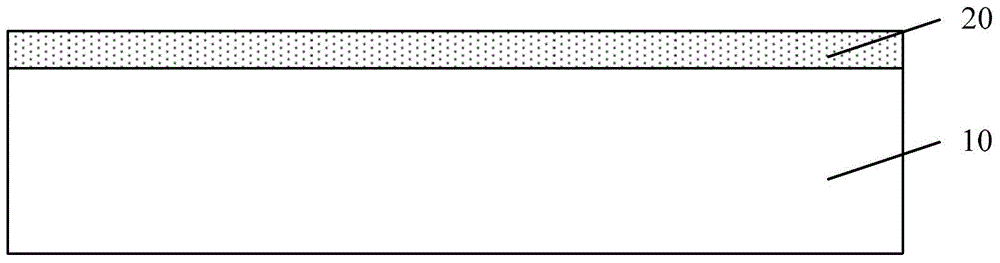
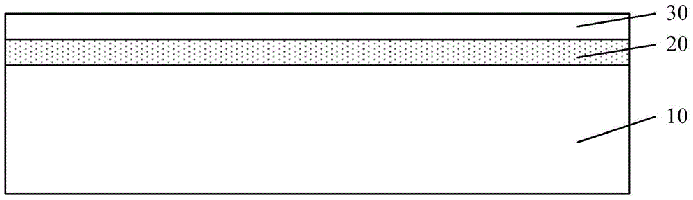
[0032] As mentioned in the background art, the quality of the interface layer formed in the prior art needs to be further improved.

[0033] Studies have found that in order to form a denser interface layer, an oxidation process is usually used to oxidize the surface of the semiconductor substrate to form an oxide layer as an interface layer. Since the thickness of the interface layer is generally thin, in order to effectively control the growth rate of the interface layer, the temperature of the oxidation process is usually lower to avoid the formation of an excessively thick oxide layer. However, the oxidation process at a lower temperature tends to cause the material of the formed interface layer to be relatively loose and have more unsaturated bonds, which affects the quality of the interface layer and ultimately affects the performance of the formed transistor.

[0034] The study found that after the formation of the interface layer, the high temperature N 2 The annealin...


PUM


Abstract

The invention provides a forming method of a semiconductor structure. The forming method includes the steps that a substrate is provided; an interface material layer is formed on the surface of the substrate through oxidation treatment; annealing treatment in an oxygen containing atmosphere is carried out on the interface material layer to form an interface layer, wherein the temperature of the annealing treatment is higher than that of the oxidation process; a dielectric layer is formed on the surface of the interface layer. By means of the method, the quality of the interface layer in the formed semiconductor structure can be improved.

Description

technical field [0001] The invention relates to the technical field of semiconductors, in particular to a method for forming a semiconductor structure. Background technique [0002] With the continuous improvement of the integration level of semiconductor devices and the reduction of technology nodes, the traditional gate dielectric layer continues to become thinner, and the leakage of transistors increases accordingly, causing problems such as waste of power consumption of semiconductor devices. In order to solve the above problems, the prior art provides a solution of replacing the polysilicon gate with a metal gate. The introduction of high-K metal gate technology has allowed the size of devices to continue to decline, allowing Moore's Law to continue. While strictly controlling the effective work function, gate leakage current, and gate size of the transistor, how to obtain an ultra-thin gate electrical thickness is the main challenge at present. [0003] The material ...

Claims


Application Information

Patent Timeline
IPC IPC(8): H01L21/28
CPCH01L21/28167H01L21/28185
Inventor 何永根禹国宾
Owner SEMICON MFG INT (SHANGHAI) CORP
Why Eureka
Try Eureka