Supercharge Your Innovation With Domain-Expert AI Agents!

Anti-substrate deformation structure

A substrate deformation and substrate technology, applied in the direction of electrical connection of printed components, printed circuit components, printed circuits connected to non-printed electrical components, etc. Achieve the effect of suppressing the deformation of the substrate

Active Publication Date: 2018-10-16
HITACHI AUTOMOTIVE SYST SUZHOU
View PDF5 Cites 0 Cited by
  • Summary
  • Abstract
  • Description
  • Claims
  • Application Information

AI Technical Summary

Problems solved by technology

[0006] Before the deformation of the substrate 100 returns to its original shape, the solder paste SP solidifies, whereby the solder paste SP connects the substrate 100, the connector base 200 and the connector terminal P together. figure 1 As shown in (c), the connector base 200 and the substrate 100 are both deformed (shape recovery) in the opposite direction to the spot welding, but also because the linear expansion coefficient of the connector base 200 is larger than the linear expansion coefficient of the substrate 100, therefore, The amount of deformation of the connector base 200 is larger than that of the substrate 100
At this time, since the solder paste SP has already connected the substrate 100, the connector base 200 and the connector terminals P, the deformation force of the connector base 200 with a relatively large deformation will be transmitted to the substrate 100 through the connector terminals P. , so that the shape of the substrate 100 recovers more than the amount of the previous deformation, so that when the connector base 200 returns to the original state, the substrate 100 deforms in the direction opposite to the direction of deformation during spot welding, and finally causes a gap between the substrate 100 and the solder paste SP. broken connection
[0007] Such deformation of the substrate 100 may not only cause failure of the electronic components mounted thereon, but may also lead to disconnection of the electrical circuit due to breakage of the solder paste SP.

Method used


Image

  • Anti-substrate deformation structure
  • Anti-substrate deformation structure
  • Anti-substrate deformation structure

Examples


Embodiment Construction

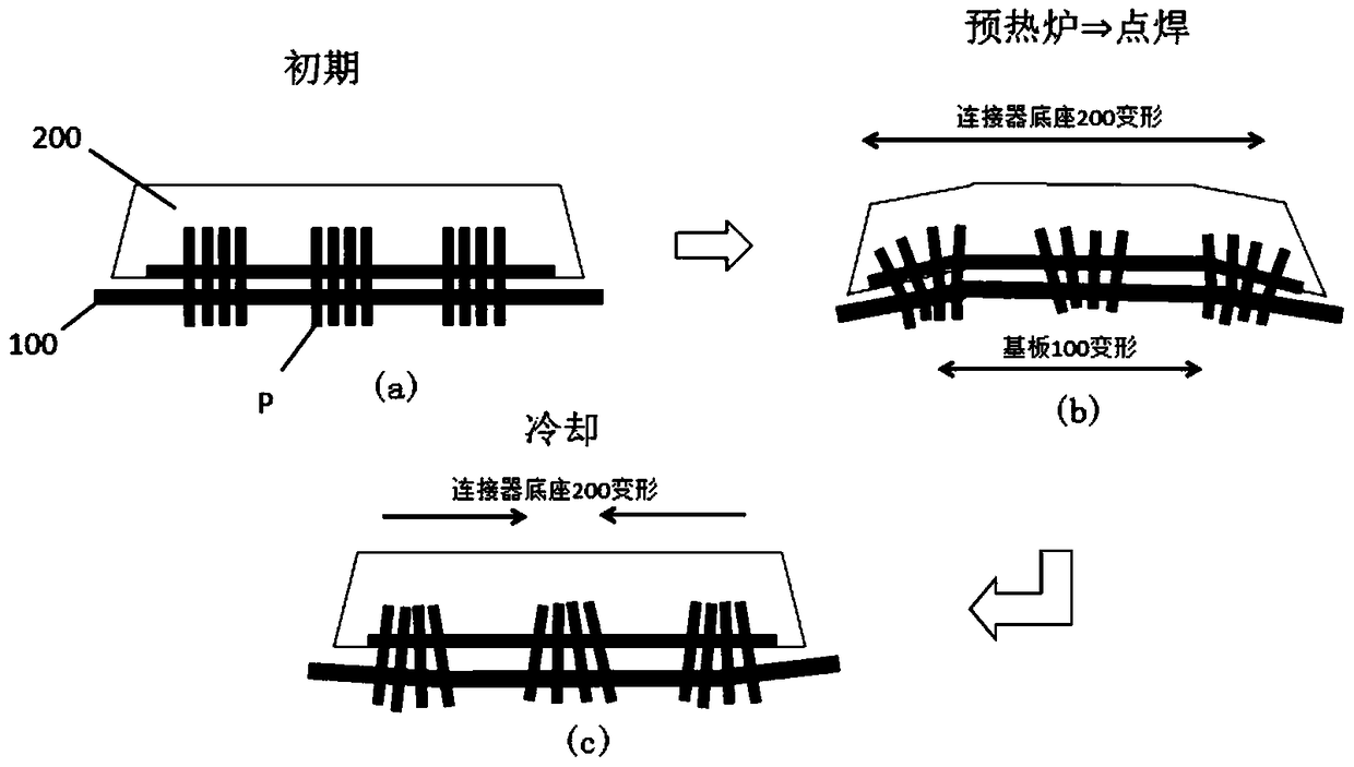
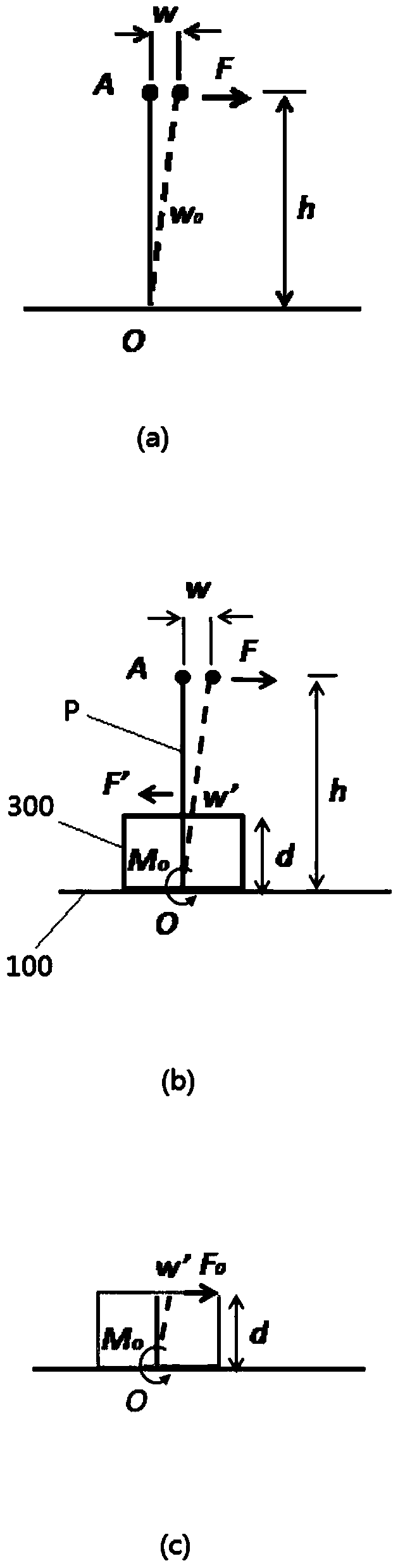
[0021] Below, refer to Figure 2 to Figure 5 , the substrate connection structure B and the force analysis in the substrate connection structure B according to the embodiment of the present invention will be described.

[0022] like figure 2 As shown in (a), the resin plate 300 is interposed between the substrate 100 and the connector base 200, and the substrate 100, the resin plate 300 and the connector base 200 are connected by 2a rows×2b columns of connector terminals P. Additionally, if Figure 5 As shown in (a), solder paste SP is applied between the resin board 300 and the connector base 200 .

[0023] Suppose the length of the resin plate is 2am, the width is 2bn, and the height is d, then as figure 2 As shown in (b), the length of the substrate 100 , the connector base 200 and the resin board 300 corresponding to a single connector terminal P is m, the width is n, and the height of the resin board 300 is d. In addition, assume that the connection point between th...


PUM


Abstract

The invention provides a substrate deformation prevention structure. With the structure, substrate deformation like warping caused by connector terminal deformation can be prevented. The substrate deformation prevention structure comprises a substrate, a connector pedestal, and a plurality of connector terminals arranged at equal intervals in an array. Besides, the structure also includes a resin plate clamped between the substrate and the connector pedestal. The substrate, the resin plate, and the connector pedestal are connected by multiple connector terminals. The thermal expansion coefficient of the resin plate is less than or equal to that of the substrate; and the thickness of the resin plate is configured to be a value to avoid substrate deformation caused connector pedestal deformation by the connector terminal.

Description

technical field [0001] The present invention relates to a structure for preventing deformation of a substrate, and more particularly, to a structure for preventing deformation of a substrate due to deformation of connector terminals. Background technique [0002] During the temperature cycle test of the ECU, it was found that the solder paste was broken when the state of the internal substrate was confirmed. After investigating the cause of solder paste cracking, it was found that when the connector is reflowed (spot soldered), thermal expansion causes the connector to be soldered to the solder paste applied with the substrate in a deformed state, and at the same time, due to the resin connector and The amount of deformation of the PCB substrate is different, so after the soldering is completed, the connector cools down and returns to its original state, but the substrate connected to the connector undergoes further deformation, causing the solder paste to break. [0003] B...

Claims


Application Information

Patent Timeline
Patent Type & Authority Patents(China)
IPC IPC(8): H05K1/02H05K1/18H05K1/11H01R12/51
Inventor 蔡亚
Owner HITACHI AUTOMOTIVE SYST SUZHOU
Features
  • R&D
  • Intellectual Property
  • Life Sciences
  • Materials
  • Tech Scout
  • Unparalleled Data Quality
  • Higher Quality Content
  • 60% Fewer Hallucinations
Learn More