Three-valued static random access memory cell realized by utilization of carbon nanotube field effect transistor

A static random storage, field effect transistor technology, applied in the field of three-value static random storage unit, can solve the problems of slowing down the writing data speed, destroying data, difficult to change the logic value of the cross-coupled inverter, etc.

Active Publication Date: 2016-11-02
NINGBO UNIV
View PDF3 Cites 8 Cited by
  • Summary
  • Abstract
  • Description
  • Claims
  • Application Information

AI Technical Summary

Problems solved by technology

But there is following problem in this SRAM cell: one, when writing operation, bit line BL and It is difficult to change the logic value stored in the cross-coupled inverter by pre-charging to the corresponding level. It is necessary to adjust the parameters of each CMOS tube, and it takes a while to write the data, which reduces the speed of writing data; 2. During the read operation, When WL is

Method used


Image

  • Three-valued static random access memory cell realized by utilization of carbon nanotube field effect transistor
  • Three-valued static random access memory cell realized by utilization of carbon nanotube field effect transistor
  • Three-valued static random access memory cell realized by utilization of carbon nanotube field effect transistor

Examples


Embodiment 1

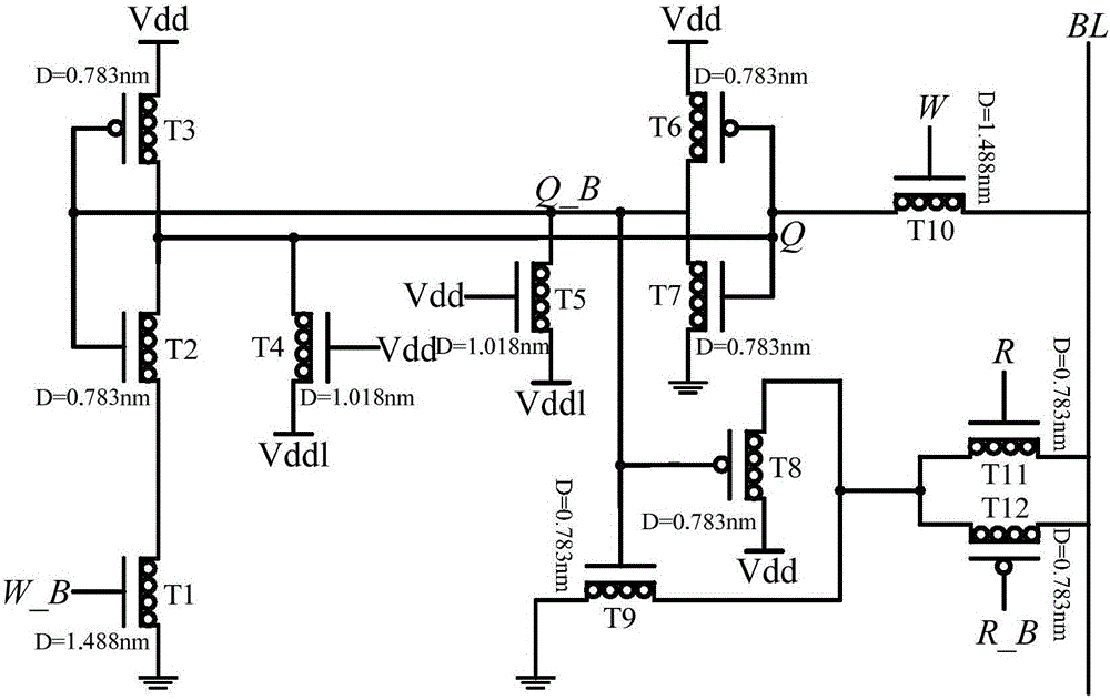
[0017] Embodiment one: if figure 2 As shown, a three-value static random memory unit realized by using carbon nano field effect transistors, including a first CNFET tube T1, a second CNFET tube T2, a third CNFET tube T3, a fourth CNFET tube T4, and a fifth CNFET tube T5 , the sixth CNFET tube T6, the seventh CNFET tube T7, the eighth CNFET tube T8, the ninth CNFET tube T9, the tenth CNFET tube T10, the eleventh CNFET tube T11 and the twelfth CNFET tube T12; the first CNFET tube T1 , the second CNFET tube T2, the fourth CNFET tube T4, the fifth CNFET tube T5, the seventh CNFET tube T7, the ninth CNFET tube T9, the tenth CNFET tube T10 and the eleventh CNFET tube T11 are N-type CNFET tubes. The third CNFET tube T3, the sixth CNFET tube T6, the eighth CNFET tube T8 and the twelfth CNFET tube T12 are P-type CNFET tubes; the source of the first CNFET tube T1, the source of the seventh CNFET tube T7 and the ninth CNFET tube The source of T9 is grounded; the drain of the first CNFE...

Embodiment 2

[0018] Embodiment two: if figure 2As shown, a three-value static random memory unit realized by using carbon nano field effect transistors, including a first CNFET tube T1, a second CNFET tube T2, a third CNFET tube T3, a fourth CNFET tube T4, and a fifth CNFET tube T5 , the sixth CNFET tube T6, the seventh CNFET tube T7, the eighth CNFET tube T8, the ninth CNFET tube T9, the tenth CNFET tube T10, the eleventh CNFET tube T11 and the twelfth CNFET tube T12; the first CNFET tube T1 , the second CNFET tube T2, the fourth CNFET tube T4, the fifth CNFET tube T5, the seventh CNFET tube T7, the ninth CNFET tube T9, the tenth CNFET tube T10 and the eleventh CNFET tube T11 are N-type CNFET tubes. The third CNFET tube T3, the sixth CNFET tube T6, the eighth CNFET tube T8 and the twelfth CNFET tube T12 are P-type CNFET tubes; the source of the first CNFET tube T1, the source of the seventh CNFET tube T7 and the ninth CNFET tube The source of T9 is grounded; the drain of the first CNFET...

Embodiment 3

[0020] Embodiment three: as figure 2 As shown, a three-value static random memory unit realized by using carbon nano field effect transistors, including a first CNFET tube T1, a second CNFET tube T2, a third CNFET tube T3, a fourth CNFET tube T4, and a fifth CNFET tube T5 , the sixth CNFET tube T6, the seventh CNFET tube T7, the eighth CNFET tube T8, the ninth CNFET tube T9, the tenth CNFET tube T10, the eleventh CNFET tube T11 and the twelfth CNFET tube T12; the first CNFET tube T1 , the second CNFET tube T2, the fourth CNFET tube T4, the fifth CNFET tube T5, the seventh CNFET tube T7, the ninth CNFET tube T9, the tenth CNFET tube T10 and the eleventh CNFET tube T11 are N-type CNFET tubes. The third CNFET tube T3, the sixth CNFET tube T6, the eighth CNFET tube T8 and the twelfth CNFET tube T12 are P-type CNFET tubes; the source of the first CNFET tube T1, the source of the seventh CNFET tube T7 and the ninth CNFET tube The source of T9 is grounded; the drain of the first CN...


PUM

PropertyMeasurementUnit
Diameteraaaaaaaaaa
Diameteraaaaaaaaaa
Diameteraaaaaaaaaa

Abstract

The invention discloses a three-valued static random access memory cell realized by the utilization of a carbon nanotube field effect transistor. The three-valued static random access memory cell comprises a first CNFET tube, a second CNFET tube, a third CNFET tube, a fourth CNFET tube, a fifth CNFET tube, a sixth CNFET tube, a seventh CNFET tube, a eighth CNFET tube, a ninth CNFET tube, a tenth CNFET tube, a eleventh CNFET tube and a twelfth CNFET tube. The first CNFET tube, the second CNFET tube, the fourth CNFET tube, the fifth CNFET tube, the seventh CNFET tube, the ninth CNFET tube, the tenth CNFET tube and the eleventh CNFET tube are N-type CNFET tubes. The third CNFET tube, the sixth CNFET tube, the eighth CNFET tube and the twelfth CNFET tube are P-type CNFET tubes. The three-valued static random access memory cell has advantages of fast read-write speed, high stability of read data, small wiring area, low power consumption and large memory capacity.

Description

technical field [0001] The invention relates to a static random storage unit, in particular to a three-value static random storage unit realized by using a carbon nanometer field effect transistor. Background technique [0002] With the development of CMOS technology and integrated circuit technology, the miniaturization of circuits brings great convenience to people's lives, and at the same time puts forward higher requirements for characteristics such as high integration and low power consumption. Especially for the issue of high integration, due to the reduction of feature size, the number of integrated components per unit chip area has increased sharply, and the feature size of integrated circuits has entered the nanometer level. In VLSI (Very Large Scale Integration, VLSI), more than 70% of the silicon area is used for wiring, which further restricts the improvement of integration. At the nanometer level, problems such as gate delay, interconnect crosstalk, and power c...

Claims


Application Information

Patent Timeline
IPC IPC(8): G11C11/419
CPCG11C11/419
Inventor 龚道辉汪鹏君张跃军康耀鹏
Owner NINGBO UNIV
Why Eureka
Try Eureka