
2.7-3.5GHz 2W GaN monolithic power amplifier and design method

A power amplifier, monolithic technology, applied in the direction of power amplifier, amplifier input/output impedance improvement, etc., can solve the problems of poor harmonic suppression, decreased stability, and poor linearity of GaN power amplifiers

Active Publication Date: 2016-11-02
成都泰格微电子研究所有限责任公司
View PDF5 Cites 5 Cited by
  • Summary
  • Abstract
  • Description
  • Claims
  • Application Information

AI Technical Summary

Problems solved by technology

[0005] Amplifiers using WIN Foundry's NP25-00 GaN process take into account the slow gain compression of GaN devices, and generally reach the maximum power or efficiency point at the 8-10dB gain compression point, so the linearity of GaN power amplifiers is poor, so the harmonic suppression also poor
The small-signal gain is about 29-31dB, which requires two stages of amplification; considering that the higher small-signal gain will lead to a decrease in stability, the amplifier is prone to self-oscillation, so it is necessary to design all levels of matching and power supply bias network very carefully , the control amplifier gain and the stability factor

Method used


Image

  • 2.7-3.5GHz 2W GaN monolithic power amplifier and design method
  • 2.7-3.5GHz 2W GaN monolithic power amplifier and design method
  • 2.7-3.5GHz 2W GaN monolithic power amplifier and design method

Examples


Embodiment Construction

[0032] Further describe the technical scheme of the present invention in detail below in conjunction with accompanying drawing:

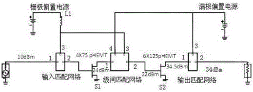
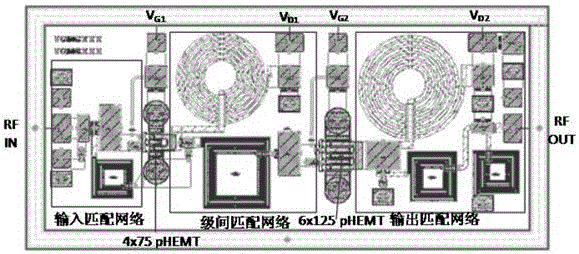
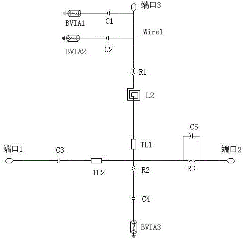
[0033] The 2.7-3.5GHz 2W GaN monolithic power amplifier is characterized in that it includes an input matching network, an interstage matching network, an output matching network, a gate bias power supply, a drain bias power supply, and pHEMT transistors S1 and S2;

[0034] The principle block diagram of the present invention, the port 1 of the input matching network is connected to the signal source, the port 3 of the input matching network is respectively connected to the port 4 of the interstage matching network and one end of the inductance L1, and the other end of the inductance L1 is connected to the gate bias power supply The positive pole is connected, the negative pole of the gate bias current is grounded, the port 2 of the input matching network is connected to the gate of the pHEMT transistor S1, the source of the pHEMT transistor S1 is gr...


PUM


Abstract

The invention discloses a 2.7-3.5GHz 2W GaN monolithic power amplifier and a design method. The amplifier comprises an input matching network, an inter-stage matching network, an output matching network and pHEMT transistors; the input matching network is connected with the inter-stage matching network through one pHEMT transistor; the inter-stage matching network is connected with the output matching network through the other pHEMT transistor; a gate bias power source is connected with the input matching network and the inter-stage matching network; and a drain bias power source is connected with the inter-stage matching network and the output matching network. According to the 2.7-3.5GHz 2W GaN monolithic power amplifier and the design method of the invention, the design difficulty of a modular circuit is simplified, the size of the modular circuit is reduced significantly compared with the size of a traditional hybrid integrated circuit; the optimal load impedance and optimal source impedance of the transistors are determined; the circuit schematic diagrams of the input matching network, the output matching network and the inter-stage matching network are designed; indexes such as a stabilization coefficient, an input and output standing wave system, gain, power, efficiency and harmonic suppression are optimized; and the layout of the monolithic microwave power amplifier is designed.

Description

technical field [0001] The patent of the present invention relates to microelectronic technology, microwave technology, semiconductor monolithic integration technology, advanced material technology and microwave power amplification technology, especially miniaturization, high efficiency, high power density monolithic microwave integrated power amplification technology, especially a 2.7 -3.5 GHz 2W GaN Monolithic Power Amplifier and Design Methodology. Background technique [0002] Monolithic Microwave Integrated Circuit (MMIC) has become an important pillar for the development of various high-tech weapons, and has been widely used in various advanced tactical missiles, electronic warfare, communication systems, land, sea and air-based various advanced Phased array radars (especially airborne and spaceborne radars) have formed rapidly in civil and commercial mobile phones, wireless communications, personal satellite communication networks, global positioning systems, direct b...

Claims


Application Information

Patent Timeline
Patent Type & Authority Applications(China)
IPC IPC(8): H03F1/56H03F3/21
CPCH03F1/56H03F3/21
Inventor 许欢
Owner 成都泰格微电子研究所有限责任公司
Learn More